

Electronics Listings
140 items found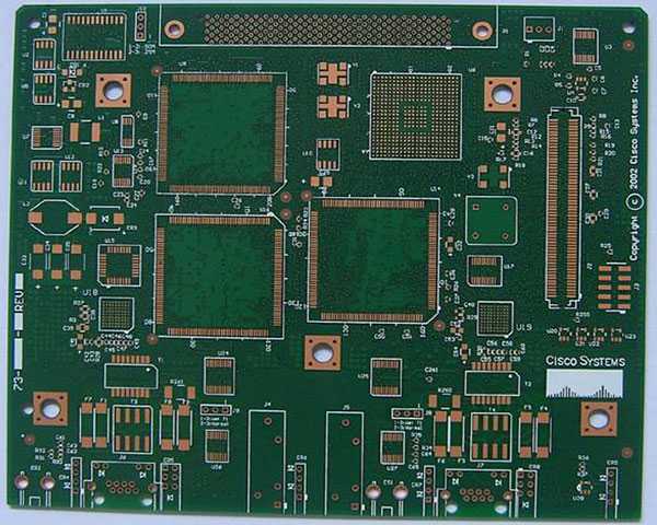
Multilayer PCB Manufacturing up to 38 Layers
Multilayer PCB Manufacturing up to 38 Layers <br>Multilayer PCB Manufacturing up to 38 layers <br> <br> <br> <br>Rigid Circuit Board Manufacturer & Assembly – One stop service PCB rigid Circuit Board is an important electronic component, support for electronic components, and a carrier for electrical connection of electronic components. Read on to learn more about multilayer PCBs, their uses and advantages in the world of modern electronics. <br> <br> <br> <br>A Multilayer Printed Circuit Board, or Multilayer PCB, is a complex circuit board composed of multiple layers of conductive material and insulating material (usually fiberglass and epoxy resin) sandwiched together. Multilayer PCB or multilayer printed circuit boards are circuit boards composed of two or more conductive layers (copper layers). The copper layer is pressed together by the resin layer (prepreg). Each layer has a conductive path or copper trace, and each layer is connected to one another through pads and vias, which act as electrical conduits. This construction allows for more complex and dense circuitry to be designed, with greater functionality and reliability compared to single- or double-sided PCBs. Multilayer PCBs are commonly used in electronic devices such as computers, smartphones, and advanced medical equipment. <br> <br> <br> <br>Multilayer PCB Prototype manufacturing <br> <br>What is Multilayer Printed Circuit Board? <br> <br> <br> <br>A Multilayer Printed Circuit Board (PCB) is a type of PCB that consists of several layers of conductive material and insulating material sandwiched together. The board is made by laminating together multiple thin layers of fiberglass or other insulating materials with copper foil. <br> <br>An integrated circuit is placed on the board, and the copper traces connected to the circuit are etched onto the inner layers of the board. The inner layers are then sandwiched together with the outer layers, forming a multilayer structure. <br> <br>Multilayer PCBs are used in high-end electronic products, such as advanced computers and mobile phones, where a high degree of density is required, and the manufacturing process is complex. They provide many benefits, including reduced size, increased reliability, and improved performance. <br> <br>Multilayer PCBs are cost-effective because they reduce the total number of components needed and improve product reliability, thus reducing the need for frequent repair services or replacement. The design flexibility of these boards also allows for more efficient use of space and improved signal routing, which aids in the performance of the product. <br> <br> <br> <br>Multilayer Printed Circuit Board stack up <br> <br> <br> <br>So what’s Multilayer PCB Benefits / Advantages? <br> <br> <br> <br>1. Increased Design Flexibility: Multilayer PCBs allow for more design flexibility and greater circuit density. With multiple layers, engineers have more space to incorporate more components and features, such as impedance control, shielding, and power planes, within the same board area. <br> <br> <br> <br>2. Increased Reliability: Multilayer PCBs are more reliable than single sided PCBs, as they are less prone to issues such as signal interference, voltage drops, and thermal stress. This is because they have a higher number of conductive layers, which allows for better shielding and more stable power distribution. <br> <br> <br> <br>3. Higher Component Density: Multilayer PCBs can accommodate a higher density of components in a smaller space while preventing signal interference. This results in a more compact and efficient design, saving manufacturers money on materials and production. <br> <br> <br> <br>4. Improved Signal Integrity: With a multilayer construction, PCBs can have better signal integrity, which means less noise and less chance of signal interference. The numerous grounds and power planes help to suppress electromagnetic interference, resulting in better connection quality. <br> <br> <br> <br>5. Better Thermal Management: Multilayer PCBs have better thermal conductivity, which reduces hot spots and improves heat dissipation. The extra layers also help to keep the heat from spreading across the board, which is important for high-power applications. <br> <br> <br> <br>6. Cost-Effective: While the initial cost of multilayer PCBs may be higher than single or double-sided PCBs, the benefits in terms of increased density, reliability, and design flexibility can mean overall cost savings in the long run. Additionally, as manufacturing techniques have evolved, the cost of producing multilayer PCBs has become more competitive. <br> <br> <br> <br>In summary, the benefits of multilayer PCBs include increased design flexibility, reliability, component density, and thermal management. They also offer improved signal integrity and can be cost-effective in the long run. These advantages make them suitable for complex electronic devices where high performance, reliability, and space-saving are required. <br> <br> <br> <br> <br> <br>-While Multilayer Printed Circuit Boards (PCBs) offer many benefits over single- or double sided PCBs, there are also some potential drawbacks to consider: <br> <br> <br> <br>1. Complexity: The multilayer PCBs are far more complex than their single-layered or double-layered counterparts. As the number of layers increases, so does complexity. This means that design and manufacturing is more challenging, which can lead to a higher cost of production. <br> <br> <br> <br>2. Cost: Multilayer PCBs are generally more expensive than single or double-layered PCBs due to their complexity. The cost of producing multilayer PCBs can increase exponentially, and the cost of manufacturing is highly dependent on the number of layers in the board, the board size, and overall complexity. <br> <br> <br> <br>3. Signal Integrity: Multilayer boards pose a higher risk of signal integrity issues due to the higher number of components and traces present in each layer. Signal interference, crosstalk, and noise can occur if proper precautions are not taken in the design process. It is therefore essential that the designer takes signal integrity into account while designing the board. <br> <br> <br> <br>4. Manufacturing Challenges: The process of cutting, etching, drilling, and laminating the multiple layers of a PCB requires highly precise equipment, which can add to the cost of manufacturing. Moreover, misalignment of layers and flaw in lamination can lead to defects that can potentially cause the PCB to stop functioning correctly. <br> <br> <br> <br>5. Environmental Impact: Multilayer PCBs contribute to electronic waste, which is a significant concern for the environment. The process of manufacturing multilayer PCBs consumes a considerable amount of energy, and the resulting waste can be toxic and difficult to recycle. <br> <br> <br> <br>Overall, Multilayer PCBs offer many advantages over single or double-sided PCBs. However, there are several issues that need to be considered during the design and manufacturing process, to achieve optimal performance. To solve your problems, here HITECH Circuits provide solutions for you. <br> <br> <br> <br>Multilayer Printed Circuit Board <br> <br> <br> <br>-Multilayer Printed Circuit Boards (PCBs) are used in a variety of applications where high performance and reliability are critical. Here are a few of the most common applications: <br> <br> <br> <br>1. Communications: Multilayer PCBs are widely used in the telecommunications industry for various applications such as cell phone base stations, satellite communications systems, and other communication devices that require high-speed data transfer rates and minimal signal loss. <br> <br> <br> <br>2. Computers: Multilayer PCBs are extensively used in computer motherboards, laptops, and other computing systems where high performance, reliability, and miniaturization are of utmost importance. <br> <br> <br> <br>3. Medical Equipment: Multilayer PCBs are a key component in many medical devices, such as imaging equipment, patient monitoring systems, and surgical instruments, where high reliability and stability are required. <br> <br> <br> <br>4. Automotive: The automotive industry uses Multilayer PCBs for applications such as engine control units, airbag systems, and lighting control systems, where reliability, durability, and efficient operation are essential. <br> <br> <br> <br>5. Aerospace and Defense: Multilayer PCBs find extensive use in aerospace and defense applications, such as missiles, satellites, and other spacecraft, where superior performance and reliability are required in extreme conditions. <br> <br> <br> <br>Overall, Multilayer PCBs are used in a wide variety of applications where increased functionality, reliability, and performance are required. With advances in technology, the use of multilayer PCBs is expected to continue to grow in the future.
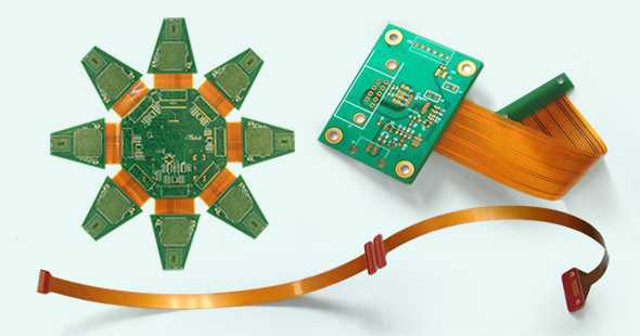
Best Flexible PCB Manufacturing
What is Flex PCB? <br> <br> <br> <br>Flexible printed circuits, also known as flex circuits, are sometimes regarded as a printed circuit board (PCB) that can bend, when in reality there are significant differences between PCB’s and flex circuits when it comes to design, fabrication and functionality. One common mistake that designers make is to design a flexible circuit using the same rules as a PCB. Flex PCB require a unique set-up and have their own set of design rules that the Hitechpcb team has termed “flex-izing” and have worked hard to perfect over the last many years. <br> <br> <br> <br>Flexible PCB, which also called Flex PCB, Flexible circuit board or flex circuit, it consists of PI base material, adhesive layer, copper layer, coverlay and sometimes with stiffeners. Flexible PCBs are now being used widely to replace traditional FR4 PCB in various different applications due to the benefits from flex PCB specially. Although more expensive than a normal rigid PCB, the right design in the right application could save weight and time in assembly, coupled with the reliability which makes flexible circuit board a worthwhile consideration. <br> <br> <br> <br>A flexible printed circuit consists of a metallic layer of traces, usually copper, bonded to a dielectric layer, usually polyimide. Thickness of the metal layer can be very thin (<.0001″) to very thick (> .010″) and the dielectric thickness can vary from .0005″ to .010″. Often an adhesive is used to bond the metal to the substrate, but other types of bonding such as vapor deposition can be used to attach the metal. <br> <br> <br> <br>flexible PCB <br> <br>How to calculate your flex pcb bend radius? <br> <br> <br> <br>Because copper tends to readily oxidize, the exposed surfaces are often covered with a protective layer, gold or solder are the two most common materials because of their conductivity and environmental durability. For non-contact areas a dielectric material is used to protect the circuitry from oxidation or electrical shorting. <br> <br> <br> <br>The number of material combinations that could go into a flexible printed circuit are nearly endless; current, capacitance, chemical and mechanical resistance, temperature extremes and type of flexing are just some of the criteria that impacts the material selections that best meet the functional needs. An experienced Hitechpcb design engineer takes the critical requirements into consideration when designing a circuit to meet your needs. <br> <br> <br> <br>Flexible printed circuit boards (FPC) has become a common component of electronic products due to its lightness and flexibility performance. It is widely used in smart terminal, wearable electronics, consumer, automotive, industrial and medical fields. The miniaturization and integrated function of electronics product development is driving FPC to fine line and multilayer design. <br> <br> <br> <br>What is Multilayer flex PCB? <br> <br>This type of flexible printed wiring boards are multilayered (with three or more conductor layers) and require plated-through holes. We could use through vias, buried vias and blind vias. <br> <br> <br> <br>A multi layer flex circuit combine several single-sided or double-sided circuits with complex interconnections, shielding and/or surface mounted technologies in a multi layer design. The multi layers may or may not be continuously laminated together throughout the production process. If your design needs require maximum flexibility, continuous lamination may not be appropriate. Multi layer circuits are an effective solution when confronted with design challenges such as: unavoidable crossovers, specific impedance requirements, elimination of crosstalk, additional shielding and high component density. You can also link here to learn more about flex pcb bending radius. <br> <br> <br> <br>Benefits to Flex PCB including: <br> <br>Assembly Error Reduction <br> <br>Decreased Assembly Time and Costs <br> <br>Design Freedom <br> <br>Flexibility during Installation <br> <br>High Density Applications <br> <br>Improved Airflow <br> <br>Increased Heat Dissipation <br> <br>Increased System Reliability <br> <br>Point-to-Point Wire Replacement <br> <br>Reliability and Durability <br> <br>Repeatable Routings <br> <br>Simplified Circuit Geometry <br> <br>Package Size and Weight Reduction <br> <br>Flex PCB Static Application <br> <br>An application where flexible circuits are flexed only to install the circuit and fit it into its application (also known as flex-to-fit or flex-to-install). A static application will typically be made using the less expensive Electro Deposited (ED) copper. <br> <br> <br> <br> <br> <br>Flex PCB Dynamic Flexing Applications <br> <br>A situation where the flexible circuit itself is dynamically (repeatedly) flexed during the actual use of the final product. Common examples include flip-type cell phones, laptops, printer heads and robotic arms. A dynamic application will require the use of Rolled Annealed (RA) copper. <br> <br> <br> <br>High Density Flex PCB Applications <br> <br>Flexible circuits allow for minutely narrow lines giving way to high density device population. Denser device populations and lighter conductors can be designed into a product, freeing space for additional product features. <br> <br> <br> <br>With a large number of investments on the facilities of flexible printed circuit board and continuously innovating the flexible circuit board manufacturing technology, Hitech Circuits is able to manufacture flexible PCBs with a great variety of technologies, from simple single sided flex PCB, double sided flex PCB to complex multilayer flexible PCB, Rigid flex pcb and support prototype FPC with laser cutting & flying probe test to mass production with toolings. <br> <br> <br> <br>Multilayer flex PCB bookbinding <br> <br>Circuit bookbinding is one of the best practices employed by Hitechpcb engineers for creating stacked PCBs. For flex PCBs, we offered a 12 layer flex PCB board with bookbinding. An additional small length is added to the circuit, making it move in an outward direction from the bend radius. There are copper traces placed at right angles to the bend. This helps restrict the circuit bend in one direction. <br> <br> <br> <br>The length to be added depends on total number of layers in the PCB, as well as the tightness of the bend. The advantage of circuit bookbinding is that it removes a great amount of tension from the various circuit layers during the bending process. The method also helps prevent buckling of the circuits at the exact bend radius. <br> <br> <br> <br>The bookbinded PCBs can easily meet the tight tolerance requirements in comparison to bonded PCBs. This is why this 12 layer flex PCB is a perfect choice for applications where stricter tolerances are required. Its polyamide construction delivers immense strength and flexibility. This flexi PCB can easily perform 180° bends. Also, the construction helps prevent buckling of inner layers, which often occurs in a long term use. This flexibility also helps reduce stress on the internal components. This 12 layer flex PCB board has better shelf life than a 12 layer bonded circuit board. The immersion gold plating offers low contact resistance, good wetting, as well as excellent shelf life. We can provide the 12 layer flex PCB board with book binding in width 4/4 mil, with minimum finish thickness 0.15 mm flex and maximum 1.6 mm. <br> <br> <br> <br>Advantages of Flexible PCB <br> <br> <br> <br>Flexible PCB technology often has a wide range of possibilities for different designs and products. <br> <br>The flexible feature is among the best attributes of the cables, wires, connectors and even PCBs. <br> <br>Some of the advantages of using the flexible circuit include: <br> <br> <br> <br>Reduces the overall weight and size. <br> <br>A flex circuit can reduce the weight of a device by up to 70%. <br> <br>Improves the packaging of electronics <br> <br>It gives you the ability to solve interconnect and packaging issues as it can bend, form and move. <br> <br>Interconnect solution as it reduces the amount of interconnects such as cables, wires, pcbs and connectors. <br> <br>Conformability as the slender nature of the material allows for making of 3D packages <br> <br>Electrical integration – You can easily come up with custom solutions basing your design on a plethora of choices of materials. Apart from that, you have the freedom to choose from the myriad of designs and plating procedures. <br> <br>Heat dissipation ability or power – The polyimide dielectric has the ability to withstand very high temperatures. You can, therefore, use it for high power applications. <br> <br>Electrical and mechanical repeatability <br> <br>Cost saving as you can save up to 30% of the total cost of hand wiring and other assembly processes. <br> <br>You can also save on space by almost 30% <br> <br>It is more reliable as it does not have any wiring errors <br> <br>Despite the numerous advantages, the flexible PCB also has its disadvantages. <br> <br>Let’s have a look. <br> <br> <br> <br>Disadvantages of Flexible PCB <br> <br>Every electronic solution must have certain demerits. <br> <br>Some of the disadvantages include: <br> <br>Flexible PCB <br> <br>A higher initial cost – Since the flex circuit is often custom for particular electronics. The initial cost of designing, photographic plate and layout is very high. This limits you to using it on large quantities to save on cost. <br> <br>Flexible circuit repairs and changes are very difficult – The initial process is not just expensive but difficult to come up with. Once you have the base map, it becomes difficult to make any more changes. Removing and replacing the covering film for repair is also extremely difficult. <br> <br>It is often small in size – The batch process of making the flexible circuits often limits the size of the flexible circuit. The production equipment limits you from making wider and longer sizes. <br> <br>Easy to damage – Improper personal operations can easily damage the flexible circuits. Rework and soldering will require the expertise of a technician. <br> <br>The process of assembly is also very difficult. <br> <br>Do not let the disadvantages kill your spirits. <br> <br> <br> <br>Why Not Make All Circuit Boards Flexible? <br> <br> <br> <br>Flexible circuit boards are certainly useful, but they are not going to replace rigid circuit boards for all applications. Cost efficiency is the main obstacle to implementing an exclusively flexible circuit board design in a consumer product. Rigid circuit boards are less expensive to manufacture and install in a typical automated high-volume fabricating facility. <br> <br> <br> <br>Typically, the ideal solution for an innovative product is one that incorporates flexible circuitry when necessary and employs solid, reliable rigid circuit boards where possible to keep manufacturing and assembly costs down. <br> <br> <br> <br>Some manufacturers even use hybrid rigid-flex printed circuit boards expressly for this purpose. This is common in laptop computers and medical devices, where rigid circuit boards can be connected to one other using ribbon-like flexible circuits. These boards can be compounded and designed to meet any number of engineering needs by focusing on the respective strengths of each circuit board base technology. <br> <br> <br> <br>Hitech Circuits creates both flexible and printed circuit boards for product manufacturers. Enjoy a consultation with one of our sales reps to find out if your product prototype design is best served by flexible or rigid circuit board types. <br> <br> <br> <br>What is Flexible PCB and Its Production Process? <br> <br> <br> <br>Flexible PCB (Flexible Printed Circuit, FPC) is very popular with excellent characteristics such as low weight and thin thickness, etc. It is also can be folded freely. Flexible PCB mainly relies on manual visual inspection with high cost and low efficiency. With the rapid development of the electronics industry, the design of printed circuit board has become more and more high -precision and high- density, traditional manual testing methods can no longer meet production needs. FPC defect automation testing has become an inevitable trend of industrial development. <br> <br>Flexible printed circuit (FPC) is a technology developed by theUnited Statesto develop aerospace rocket technology in the 1970s. It is high reliability, excellent deflection made by polyester film or polyimide as a substrate material. A flexible circuit is formed by embedding a circuit design in a thin, flexible plastic sheet that is flexible, allowing a large number of precision components to be stacked in a narrow and limited space. This circuit can be bent and folded at will. Flexible has the characteristics like light weight, small size, good heat dissipation, easy installation, etc, it breaks through the traditional interconnection technology in the structure of the flexible circuit, the material is composed of insulating film conductor and adhesive <br> <br> <br> <br>Flexible PCB includes single sided FPC, double sided FPC and multilayer FPC, etc. Single FPC has chemically etched conductive pattern layer, the conductive pattern layer on the surface of the flexible insulating substrate is calendered copper foil. The insulating substrate may be polyimide, polyethylene terephthalate, arylamide fiber ester and polyvinyl chloride. The double sided FPC on both sides of the insulating base has a conductive graphics made of etching, which increases the wiring density of the unit area. Metal hole connects the graphic connection on both sides of the insulation material to form a conductive pathway to meet the flexible design and function. The covering film can protect the single, double -sided wire and indicate the position of the component placed. According to demand, metal holes and coverage layers are optional. This type of Flexible PCB has fewer applications. Multi -layer flexible PCB is to press the single-sided or double-sided flexible circuit layer of 3 or more layers together. The metal hole is formed by drilling and electroplating, and conductive channels are formed among different layers. In this way, there is no need to use a complex welding process. Multi-layer circuits have huge functional differences in higher reliability, better thermal conductivity and more convenient assembly performance. <br> <br> <br> <br>At present, the production process of flexible PCB mainly includes looping, Sizing conductor, etching, routing of the conductors, ground planes, sizing of the holes, filleting, button plating, adhesive-backed films, screen-print liquid overcoats, photo imaginable liquid, film polymers and other processes. See the figure for the specific production process.
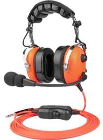
PNR Aviation Headset
#FNBV57 <br>A PNR (Passive Noise Reduction) aviation headset is a type of headset specifically designed for pilots and aviation professionals who require effective noise reduction during flights. PNR headsets utilize passive noise reduction techniques to minimize the impact of external noise on the user's hearing. With a specialized earcup for noise-proof insulation, it's worked by mechanically blocking sound waves from entering the ear. With NNR of 23dB, it's a perfect choice for aviators. <br> <br>What Is The Difference Between PNR And ANR Headset? <br>The terms pnr aviation headset and ANR refer to two different types of headsets commonly used in aviation and other noise-intensive environments. Here's a breakdown of their differences: <br>PNR (Passive Noise Reduction) Headset: <br>PNR headsets are equipped with passive noise reduction technology. They use physical materials and design features to block out external noise. The primary components of PNR headsets are ear cups with sound-absorbing foam padding and a tight seal around the ears. The foam absorbs and dampens the ambient noise, reducing its impact on the user's ears. <br>Pros of PNR headsets: <br> <br>Affordability: PNR headsets are more budget-friendly than ANR headsets. <br> <br>Durability: PNR headsets are known for their sturdy construction and ability to withstand wear and tear. <br> <br>Reliability: PNR headsets do not rely on batteries or electronics, making them less prone to power-related issues. <br> <br>Lower power consumption: PNR headsets don't require power, making them suitable for situations with limited power sources. <br> <br>Cons of PNR headsets: <br>They do not eliminate noise completely, as some sound can still leak in. <br>They are less effective in reducing low-frequency noise. <br>May cause ear discomfort during extended use due to the tight seal. <br>Relatively simple and less expensive compared to ANR headsets. <br> <br>No reliance on electronics or batteries, making them more reliable. <br> <br>Provide a consistent level of noise reduction across different frequencies. <br> <br>ANR (Active Noise Reduction) Headset: <br>ANR headsets utilize active noise cancellation technology. They incorporate microphones on the outside of the ear cups that detect ambient noise. The headset then generates an "anti-noise" signal that is precisely out of phase with the detected noise. When the anti-noise signal combines with the ambient noise, they cancel each other out, resulting in reduced noise levels reaching the user's ears. <br>Pros of ANR headsets: <br> <br>Effective noise cancellation: ANR headsets use active technology to cancel out external noise, providing a quieter listening experience. <br> <br>Enhanced comfort: ANR headsets are designed with ergonomic features and cushioning for a more comfortable fit during extended use. <br> <br>Customizable noise cancellation: ANR headsets often offer adjustable noise cancellation levels, allowing users to control the amount of noise reduction based on their preference and the surrounding environment. <br> <br>Improved audio clarity: By reducing background noise, ANR headsets enhance the clarity and intelligibility of audio communication and entertainment. <br> <br>Cons of ANR headsets: <br>ANR headsets are generally more expensive due to the added technology. <br> <br>They require batteries or power source to operate the active noise cancellation circuitry. <br> <br>Some ANR headsets may introduce slight audio artifacts or a faint "hissing" sound due to the cancellation process. <br> <br>Highly effective in reducing both low-frequency and high-frequency noise. <br> <br>Offer superior noise reduction compared to PNR headsets. <br> <br>Provide a more comfortable listening experience as they don't rely solely on physical pressure around the ears. <br> <br>In summary, PNR headsets use passive methods like foam padding and a tight seal to reduce noise, while ANR headsets employ active noise cancellation technology to actively counteract ambient noise. ANR headsets generally offer higher noise reduction capabilities, but they come at a higher cost and rely on batteries or power. The choice between PNR and ANR headsets depends on personal preference, budget, and the specific noise environment in which they will be used. <br> <br>Key Features of PNR Headsets <br>PNR (Passive Noise Reduction) headsets offer several key features that contribute to their effectiveness in reducing external noise. Here are some of the important features you can expect to find in a PNR headset: <br> <br>Ear Cups: PNR headsets typically have large ear cups that encompass the ears entirely. The ear cups are designed to provide a secure fit and create a seal around the ears, preventing external noise from entering. <br> <br>Sound-Absorbing Padding: The ear cups of PNR headsets are lined with sound-absorbing padding or foam. This padding helps absorb and dampen ambient noise, reducing its impact on the user's ears. <br> <br>Sealing: PNR headsets employ a sealing mechanism to enhance noise reduction. The ear cups are designed to fit snugly around the ears, effectively blocking out external sounds and creating a quieter listening environment. <br> <br>Adjustable Headband: PNR headsets typically feature an adjustable headband that allows users to customize the fit according to their head size and comfort preferences. The headband ensures a secure and comfortable fit during extended use. <br> <br>Boom Microphone: Many PNR headsets come with a boom microphone attached to one of the ear cups. The boom microphone allows for clear voice transmission and communication with air traffic control or other personnel. <br> <br>Volume Control: PNR headsets often have built-in volume control options. These controls enable users to adjust the audio output to their desired level, ensuring clear communication and comfortable listening. <br> <br>Durability: PNR headsets are designed to withstand the demanding conditions of aviation environments. They are typically constructed using durable materials that can withstand frequent use, rough handling, and exposure to various elements. <br> <br>Weight and Comfort: PNR headsets aim to provide a balance between noise reduction and comfort. They are designed to be lightweight and ergonomic, minimizing discomfort during prolonged use. <br> <br>Compatibility: PNR headsets are compatible with standard aviation audio systems and intercom systems commonly used in aircraft. <br> <br>It's important to note that the specific features and design may vary among different models and brands of PNR headsets. It's recommended to review the specifications and features of a particular headset before making a purchase to ensure it meets your specific needs and preferences. <br> <br>Ray talk, as an excellent call center head set manufacturer, offers a wide range of call center head set for you to choose from. <br> <br> <br> <br>[a]https%3A%2F%2Fwww.raytalkcomms.com%2Fproducts%2Fpnr-aviation-headset%2F[/a]
3.0mm Connector
Connectors are crucial components in electronic devices, ensuring seamless power and data transmission. The 3.0mm connector is widely used in various applications due to its robust design and reliable performance. This connector size is ideal for power supply connections in devices that require a stable and strong connection. Its larger size compared to other connectors allows it to handle higher currents, making it suitable for power-intensive applications such as industrial equipment and large household appliances. The 3.0mm connector's durability and ability to maintain a secure connection even in demanding environments make it a popular choice for engineers. <br>In contrast, the 0.8mm connector is known for its compact size, making it perfect for applications where space is at a premium. This type of connector is commonly found in mobile phones, tablets, and other compact electronic devices. Despite its small size, the 0.8mm connector offers reliable performance and ensures stable connections. Its design allows for high-density configurations, which is crucial in modern electronic devices that are becoming increasingly compact. The precision engineering behind these connectors ensures that they can handle the rigorous demands of portable electronics, including frequent plugging and unplugging. <br>The 1.25mm connector strikes a balance between the 3.0mm and 0.8mm connectors, offering a medium size that provides both versatility and reliability. This connector is often used in applications like computer peripherals and small household electronics. The 1.25mm connector is favored for its ability to provide stable connections while maintaining a relatively small footprint. Its versatility makes it suitable for a wide range of applications, from data transmission in computer networks to connecting components within various electronic devices. The 1.25mm connector's blend of size, reliability, and performance ensures it remains a staple in many electronic designs.
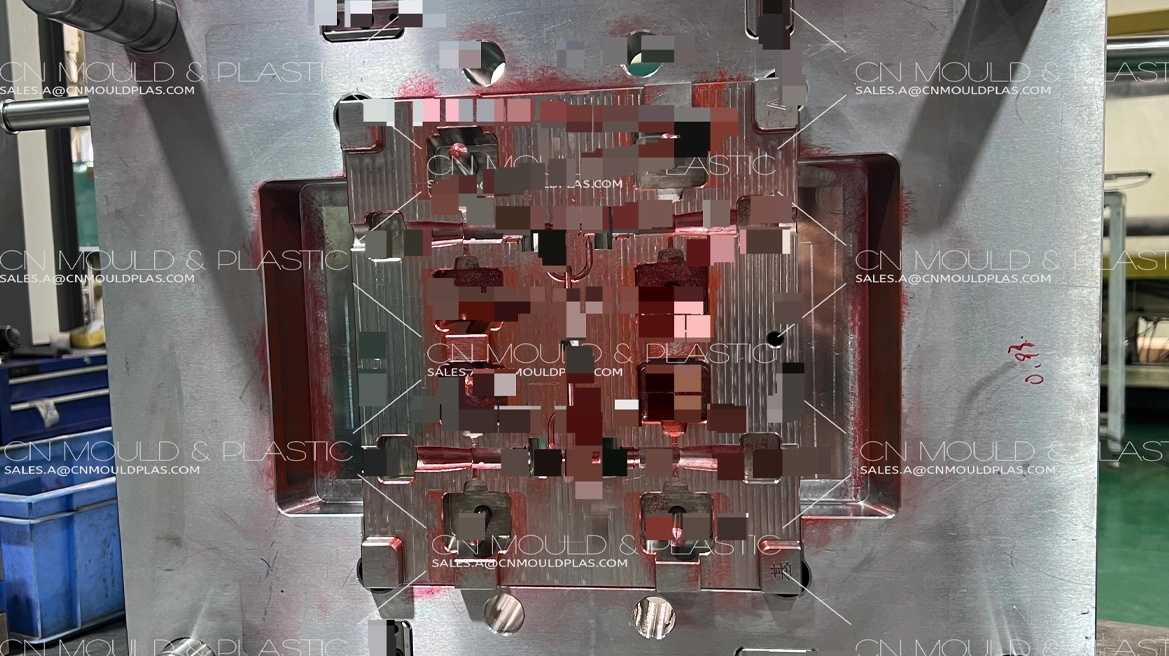
LOW PRESSURE Molding
#insert #molding <br>LOW PRESSURE Molding <br>As the name suggests, low pressure molding, low pressure forming is a process that injects materials into a mold with very low injection pressure and solidifies quickly. <br> <br>Low pressure injection molding typically involves the use of an insert, rather than solely injecting a product. Molten plastic is then injected into the mold cavity at a low pressure. Once the plastic has cooled, the insert is fused with the plastic to form a cohesive plastic component. <br> <br>WHY CHOOSE <br>CN Low Pressure Molding <br>1. We offer comprehensive low pressure injection molding solutions that cover everything from design for manufacturing to DFM, mold design and fabrication, materials selection, equipment, and process parameter optimization. <br> <br>2. Possess a high-performance low pressure molding systems that can meet your product needs. <br> <br>3. Our company possesses a professional design team that provides technical support throughout the production process for you. <br> <br>4. Get certified with ISO 9001:2015 and IATF 16949:2016 to ensure the quality of your products. <br> <br>#APPLICATION <br>LOW PRESSURE MOLDING Application <br>Low pressure injection molding is distinguished from traditional injection molding by its lower injection pressure. This feature offers the advantage of reducing the likelihood of damaging the encapsulated parts. As a result, low pressure moulding processes find primary use in two distinct applications: <br> <br>1. In electronic and electrical industry: printed circuit boards, automotive electronic products, sensitive components, mobile phone batteries, cables, connectors, sensors, etc. <br> <br>2. In automotive industry: door guard plates, column guard plates and wrap frame guard plate covered with skin such as fabric, PVC fabric. <br> <br>Low Pressure Molding Application <br>#ADVANCED LOW PRESSURE MOLDING <br>HOW DOES <br>Low Pressure Molding Work? <br>How Does Low Pressure Molding Work? <br>Step 1 : Put the electronic parts into the predetermined mold cavity. <br> <br>Step 2 : Use low pressure to inject plastic, then apply low pressure molding using a machine for Overmolding. <br> <br>Step 3 : After cooling, remove the plastic parts manually and inspect them. <br> <br>#ADVANCED MANUFACTURING <br>THE DIFFERENCE BETWEEN Low Pressure Molding And LSR Molding <br>Low pressure molding (LPM) and injection molding are both popular manufacturing processes for creating plastic parts, but they have some key differences in terms of materials, processes, applications, and advantages. Here's a comparison: <br> <br>Material: <br> <br>LPM uses a limited range materials, like PO, PP, PA, and even epoxy and polyurethane.Injection molding primarily uses thermoplastic materials that can melt and re-solidify, such as PP, PE, ABS, and PS. <br> <br>Process: <br> <br>LPM utilizes moderate pressure (around 3.5-14 bar) to inject molten plastic into a mold cavity. Injection molding employs high pressure (150-3000 bar) to rapidly inject molten plastic into a closed mold cavity under high pressure, then cools and solidifies it. <br> <br>Applications: <br> <br>LPM is often used for simpler parts where high precision is not critical.Injection molding is best suited for complex, high-precision parts requiring tight tolerances and intricate details, like gears, housings, electronic components, and medical devices. <br> <br>Summary: <br> <br>LPM molds are generally less expensive than injection molding molds due to their simpler design and lower pressure requirements. <br> <br>LPM offers more flexibility in material selection, while injection molding offers better control over material properties. <br> <br>Both processes are capable of high throughput, but injection molding can achieve faster cycle times for complex parts. <br> <br>Surface finishes can be comparable for both methods, but injection molding offers a nicer and wider range of finishing options. <br> <br>Ultimately, the best choice between LPM and injection molding depends on your specific project requirements and priorities. <br> <br>#ADVANTAGES <br>EXPLAIN ADVANTAGES OF Low Pressure Molding <br>RELIABLE <br>The low pressure molding product offers effective defense against water, dust, chemicals, shock, vibration, and high temperatures, and superbly relieves pressure. <br> <br>QUICK <br>Simplify the production process, cut production time, increase productivity, reduce the rejection rate, and lower production costs. <br> <br>ECO-FRIENDLY <br>Choose materials that are eco-friendly, reduce the use of unnecessary materials, and minimize material waste. <br> <br>#LOW PRESSURE MOLDING MATERIALS <br>MATERIALS OPTION OF CN's Low Pressure Molding <br>Low pressure molding is a great method to protect sensitive components. The type of plastic used is crucial because it impacts the strength, durability, and thickness of the final product. Thus, it's essential to select the right materials for different application, as outlined below: <br> <br>1. For automotive electronic parts, It is advisable to utilize materials that can withstand high temperatures as the surrounding temperature can be quite elevated. <br> <br>2. For outdoor electronics, such as wearable devices, bicycle components, underwater devices, or sensors, it may be necessary to use materials with a higher viscosity. <br> <br>In CN, the most commonly used material for low-pressure molding is polyamide (PA). It is chosen because of its high mechanical properties and melting point. In particular, components produced from PA materials display exceptional durability against wear and tear, possess natural lubrication capabilities, and exhibit strong resistance to fatigue. <br> <br>Now tthe price of injection molding mold is reasonable, if you have needs, please contact us. <br> <br>[a]https%3A%2F%2Fwww.cnmouldplastic.com%2Flow-pressure-molding%2F[/a]
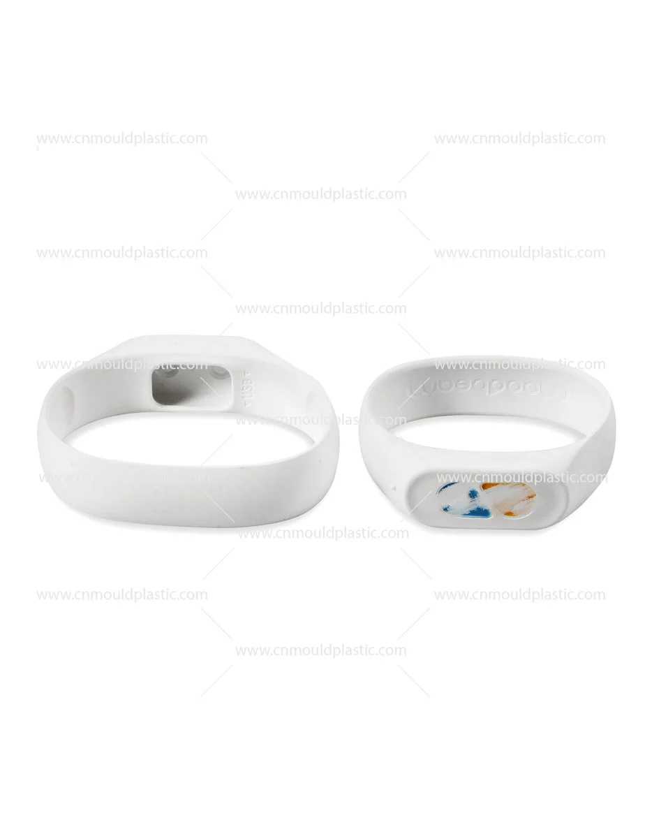
LSR Molding
#multi #injection #molding <br> <br>LSR Molding <br>Liquid Silicone Rubber(LSR) has been in high demand since its development in these days. That's hardly surprising given its physical properties and the variety of applications it may serve. LSR is long-lasting, flexible, stable, and versatile. Customers appreciate the dependability and quality that our company consistently provides, so it's no wonder that our influence in the LSR sector is expanding as well. <br> <br>Injection moulding of liquid silicone rubber is a process that involves mixing two-part Liquid Silicone Rubber material, then curing it thermally in a mold using a platinum catalyst to produce silicone rubber parts and products. <br> <br>Liquid Silicone Rubber Molding is quite similar to the traditional process of plastic injection molding. However, the primary distinction between the two methods is that the conveying system for materials is cooled while the mold is heated. <br> <br>CN: The Perfecting LSR Process <br>STEP1 <br>Put the base-forming silicone and the platinum catalyst parts of the Liquid Silicone Rubber compounds A & B into the pumping system using the supply drums. Additionally, there is a separate container for the additives and color pigments. <br> <br>STEP2 <br>Mix the two Liquid Silicone Rubber, base-forming silicone and platinum catalyst by using the metering unit. Make sure that the two Liquid Silicone Rubber are kept at a consistent ratio of 1:1 while being transported simultaneously. <br> <br>STEP3 <br>Set up and start machine, Inject these mixed compounds into the mold cavity via nozzle and cold runner system. <br> <br>STEP4 <br>Once the silicone rubber products have undergone vulcanization and solidification, they can be removed from the mold either automatically or manually. <br> <br>STEP5 <br>The product will be post-processed and inspected. <br> <br>#APPLICATION <br>LSR MOLDING Application <br>Liquid Silicone Rubber is a material that extremely wide applications, suitable for numerous applications in various industries including medical, life sciences, automotive, consumer goods, and industrial products. <br> <br>Medical & Health: Medical tube, Endoscope components, Breathing face mask, Laryngeal mask; <br> <br>Automobile: Gasket, O-Ring, Seals, Optical coupling LED lens; <br> <br>Optics: Exterior and professional Lighting; <br> <br>Electronics: LED lens, protective cases, Watch bands, Silicone Lightning Cable; <br> <br>Consumer goods: Earphone, Earplugs, Eyeglass Nose Pads, safety goggles; <br> <br>Babies & Kids: Silicone baby bottles, Silicone pacifier, Silicone baby toothbrush. <br> <br>In short, there are numerous products that can be manufactured through the process of liquid silicone molding . <br> <br>WHY CHOOSE CN LSR Molding <br>EXTENSIVE EXPERIENCE <br>For almost 20 years, CN Mould & Plastic Limited has focused on making injection molds and doing injection molding. CN are fully knowledgeable about the LSR molding process and can handle problems that other companies might not be able to handle. <br> <br>HIGH EFFICIENCY <br>We are capable of creating prototypes for your parts within a short time frame. This speedy prototyping process enables you to swiftly enhance your parts and commence the production of components promptly. <br> <br>CUSTOMIZATION <br>Our team of engineers can assist you in selecting the appropriate type of LSR for your project, producing the products you require. We offer a complete range of services, including mold design, production, assembly, and coordination throughout the entire process. <br> <br>QUALIFICATIONS <br>CN has been certified in Quality Management by the International Organization for Standardization (SGS) according to the ISO 9001:2015 and IATF 16949:2016 disciplines. <br> <br>CRITICAL ADVANTAGES OF <br>LSR Molding <br>Advantages of LSR Molding <br>LSR's versatility and impressive properties make it a valuable material for a wide range of applications. From everyday gadgets to cutting-edge medical devices, LSR is shaping the future in many ways. <br> <br>Crystal Clear and Tough: LSR boasts excellent transparency, allowing intricate details to shine through. It's also tear-resistant, meaning it can handle wear and tear without breaking easily. It even resists turning yellow over time, keeping your products looking fresh. <br> <br>Temperature Hero: This material is truly extreme temperature resistant, functioning well even in extreme temperatures ranging from -60°C to 250°C. So, whether you're dealing with icy winters or scorching summers, LSR can handle it. <br> <br>Durable and Dependable: Strong, flexible, and stable, LSR offers long-lasting performance. It can even act as an insulator, preserving both electrical and thermal conductivity when needed. <br> <br>Automotive Applications: In the automotive world, LSR shines due to its heat resistance, ability to compress without losing shape, and excellent resistance to chemicals. It's commonly used in sensor covers, seals, and even interior components. <br> <br>Beyond Cars: LSR's chemical resistance and ability to withstand extreme temperatures make it popular in consumer electronics too. You'll find it in things like remote control buttons, phone cases, and even smartwatch bands. The growing popularity of wearable tech is expected to further boost the demand for LSR in this industry. <br> <br>Medical Marvel: Because LSR is highly inert, biocompatible, and hypoallergenic, it's safe for use in medical devices like prosthetics and even artificial organs. However, it's important to note that it can degrade in highly acidic environments. <br> <br>#ADVANCED LSR MOLDING <br>HOW DOES LSR Molding Work? <br>STEP1 <br>Put the base-forming silicone and the platinum catalyst parts of the Liquid Silicone Rubber compounds A & B into the pumping system using the supply drums. Additionally, there is a separate container for the additives and color pigments. <br> <br>STEP2 <br>Mix the two Liquid Silicone Rubber, base-forming silicone and platinum catalyst by using the metering unit. Make sure that the two Liquid Silicone Rubber are kept at a consistent ratio of 1:1 while being transported simultaneously. <br> <br>STEP3 <br>Set up and start machine, Inject these mixed compounds into the mold cavity via nozzle and cold runner system. <br> <br>STEP4 <br>Once the silicone rubber products have undergone vulcanization and solidification, they can be removed from the mold either automatically or manually. <br> <br>STEP5 <br>The product will be post-processed and inspected. <br> <br>#FAQS <br>FAQ OF Liquid Silicone Rubber Molding <br> <br>What is Liquid Silicone Rubber? <br> <br>Liquid Silicone Rubber is an organic silicone material that is transparent, non-toxic, heat-resistant, highly resilient and flexible once it has set. When it undergoes sulfurization, it exhibits low viscosity, quick curing, shear thinning, and a high coefficient of thermal expansion. <br> <br>Liquid Silicone Rubber is a two-component material that has high transparency, strength and tear resistance. It can be processed through liquid silicone injection molding processes. <br> <br>The Characteristics of LSR <br> <br>Biocompatibility: After extensive experiments, it has been found that LSR is highly compatible with human tissues and fluids. In contrast to other elastomers, LSR is less prone to bacterial growth and does not cause contamination or corrosion of other materials. <br> <br>Chemical Resistance: LSR can withstand water, oxidation, and certain chemical solutions like acids and bases. <br> <br>Temperature Resistance: Compared to other elastomers, LSR can tolerate a variety of high/low temperature restrictions. <br> <br>Mechanical Properties: The LSR material has great stretchability, strong resistance to tearing and pulling, and remarkable flexibility. Its hardness can range from 5 to 80 Shore A. <br> <br>Electrical Properties: LSR has great insulation properties and is a great choice for many electrical applications. Silicone can withstand both higher and lower temperatures compared to traditional insulation. <br> <br>Transparency and Pigmentation: LSR has a natural transparency that allows for the production of colorful and customizable molded products. <br> <br>Now tthe price of china injection molding mold is reasonable, if you have needs, please contact us. <br> <br>[a]https%3A%2F%2Fwww.cnmouldplastic.com%2Flsr-molding%2F[/a]
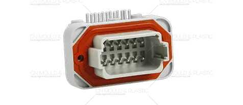
INSERT Molding
#injection #molding #exporter <br>INSERT Molding <br>Insert molding is a particular subset of injection molding used specifically to fuse many materials into one finished product. Therefore, the fundamental principle of custom insert molding is the same as that of injection molding. <br> <br>A pre-prepared insert is inserted in the mold by hand or by machine at the correct location, followed by the injection of molten plastic into the mold cavity. The insert is joined with the cooled and solidified plastic to create the final product once the mold is opened. With the help of this insert injection technique, the parts characteristics can be improved along with its overall stability. As a result, insert injection molding has been an increasingly common injection process in recent years. Typical example of insert molding applications is connector housing that combines machined metal pins with plastic. <br> <br>TYPES OF Insert Molding From CN <br>Stamped Parts Insert Molding <br>Angled Pins Insert Molding <br>POGO Pins Insert Molding <br>Magnet Insert Molding <br>PCB Insert Molding <br>Metal Insert Molding <br>Rubber Insert Molding <br>Silicone Insert Molding <br>Micro Insert Molding <br> <br>#ADVANCED MANUFACTURING <br>WHY CHOOSE CN Insert Molding <br>Extensive Experience <br>EXTENSIVE EXPERIENCE <br>Over 20 years, CN Mould & Plastic focus on making injection mold and develop an expertise of Elastomers. Tens of Millions of parts are shipped out each year to world-class customer such as HP, DELL, Apple. <br> <br>Development Advantage <br>DEVELOPMENT ADVANTAGE <br>Rich experience in injection molding and design flexibility for insert molding enable CN to quickly comprehend your need, cooperate with you to develop and improve products, and satisfy your customized requirements. <br> <br>Quality Assurance <br>QUALITY ASSURANCE <br>CN is certified by ISO 9001:2015 and ATF 16949:2016 discipline issued by the International Organization for Standardization (SGS) for Quality Management. Besides, we have a systematic program for handling complaints. <br> <br>Timely Delivery <br>TIMELY DELIVERY <br>Once we receive the customer's order, we will arrange the production as soon as possible. <br> <br>Our production philosophy is to achieve machine automation as much as possible, putting efficiency and quality in an important position to ensure timely delivery. <br> <br>#APPLICATION <br>INSERT MOLDING Application <br>If you need a high-quality, complex product, insert molding is a most efficient method that bonds effectively between plastic and inserts made from other materials. In particular, this process is ideally suited for the production of parts with extremely tiny tolerances and mass production. <br> <br>Because of this, insert molding technology has found increasing use in industries such as automotive, medicine, and consumer electronics in recent years. SIM card holders, connectors, charger housings, electrical wire connectors, and so on are all examples of common products made with insert molding. <br> <br>WHAT MATERIALS CAN BE USED IN INSERT MOLDING? <br>To precisely manufacture a plastic product via the injection molding process, a very tight tolerance is required. The molding process can fail even if there is only a tiny difference. Therefore, it is essential to know the shrinkage rate of the injecting material. Injecting materials for CN are usually chosen from nylon, PBT, and PPS. <br> <br>Materials for the insert need to be able to sustain the pressure of the injection molding process without being deformed; thus, metal, plastic, silicone, magnet, cable are all appropriate insert materials. In CN Mould, the insert molding process is widely applied to automotive accessories and electronic components, such as connector housing, charger housing, SIM card holders, cable components, etc. Therefore, metal is the most common material for inserts, for example, copper brass part, stamped part, angled pin, pogo pin. Of course, there are some special materials, like PCB. <br> <br>FAQ OF Insert Molding <br> <br>What's Insert Molding? <br> <br>Insert molding technology combines plastic with other different materials to form a single product. This may include combinations of plastic and metal, plastic and stamped insert, plastic and magnet, and so on. <br> <br>The Advantage of Insert Molding? <br> <br>1. Increase Design Flexibility. <br> <br>2. Reduces Assembly and Labor Costs. <br> <br>3. Increases Reliability. <br> <br>4. Reduces Size and Weight. <br> <br>When to Use Insert Molding? <br> <br>1. When using prefabricated substrates. <br> <br>2. If the substrate contains metal, cable, stamped part, or PCB. <br> <br>Note When Designing the Insert Molding Mold? <br> <br>1. Limiting tests for the part's shape and dimensional accuracy is crucial due to the inconsistent shrinkage rates of the materials during the insert molding process. <br> <br>2. Inserts can be deformed and shifted during the injecting process; therefore, it is necessary to fully take into account the shape of products and the position of inserts when designing the mold. <br> <br>3. Predicting gate location and molding cycle in advance is required. <br> <br>4. Confirming whether the insert requires pre-heating or drying treatment is necessary for ensuring both the quality of the finished product and the stability of the molding process. <br> <br>As one of insert molding manufacturers and insert molding suppliers, we will do our best to meet all the needs of customers. <br> <br>If you are looking for a reliable china injection mold factory, please choose us, and we will be your best partner. <br> <br> <br>[a]https%3A%2F%2Fwww.cnmouldplastic.com%2Finsert-molding%2F[/a]
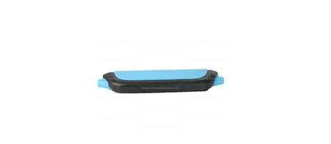
MULTI-SHOT Molding
#injection #molding #cost <br>Multi Shot Molding <br>Different plastic materials and colors are used to create multi shot injection molding parts. In the process of injection molding, different materials must be tightly differentiated from one to another and cannot penetrate one another, like a Heart Rate Band. <br> <br>Different injection molding goods need to match different types of plastic materials in addition to materials with diverse hues, such as: <br> <br>1) The majority of the time, thermoplastic material and thermoplastic elastomer (such as TUE, TPU, etc.) are used to create products that combine soft and hard components. The product may have a rigid, corrosion-resistant matrix as a result of this combination, as well as a sealed anti-seismic or more pleasant feel. <br> <br>2) Items that incorporate Liquid Silicone Rubber (LSR). Since LSR has greater temperature resistance and mechanical qualities than thermoplastic elastomer, it is being used more frequently in multi material injection molding processes. <br> <br>#ADVANCED MANUFACTURING <br>WHY CHOOSE CN Multi-Shot Molding <br>1 <br>CN Mould & Plastic Limited launches its mold business in 2006 after more than 20 years of expertise in the production of injection molds. We are a multi shot injection molding factory and molder with expertise in Dual Shot Molding, Overmolding, and Insert Molding. Our skilled mold makers can offer high-quality, all-in-one service and injection mold creation. <br> <br>2 <br>Insert Molding and Overmolding are strong points of CN Mould & Plastic Limited. We frequently offer our customers product design recommendations as a way to improve Overmolding. CN Mould & Plastic Limited provides full-service contract manufacturing and has a design and development team for molding and tooling. In order to face each obstacle, we've been paying attention to what our clients desire and will keep developing our capabilities. <br> <br>3 <br>CN Mould & Plastic Limited has received certification for meeting the worldwide standards for the quality system in the medical industry, ISO 9001:2015 and IATF 16949:2016. CN Mould & Plastic Limited produces molds for a variety of sectors and provides services to the USA, Canada, and Europe. The largest tool is up to 1.3 meters in length. <br> <br>4 <br>With imported EDM and high-speed CNC precision process machines, CN Mould & Plastic Limited will check color, appearance and tolerance through quality control at every stage of the manufacturing process. We can assist you in creating any type of injection mold, even one with intricate structures. During the creation of injection molds, strict quality control is also utilized. <br> <br>MATERIALS OPTION OF <br>CN's Multi-Shot Tooling <br>Because it directly affects a number of factors, such as mold manufacturing technique, mold life, the quality of plastic components made from molds, and mold processing costs, the choice of mold materials is an important stage in the design and manufacture of molds. <br> <br>In general, between 150 and 200 °C in both temperature and pressure are needed to operate plastic molds. Taking into account the various usage scenarios and processing methods of plastic mold, the following are the fundamental performance characteristics of steel for plastic mold that CN Mould & Plastic Limited selected: <br> <br>Materials Option of CN's Multi-Shot Tooling <br>Stable thermal performance. <br> <br>Excellent machinability. <br> <br>Corrosion protection. <br> <br>Outstanding polishing results. <br> <br>Strong fatigue and wear resistance. <br> <br>Sufficient surface hardness. <br> <br>MULTI-SHOT MOLDING Application <br>Multi injection molding has been employed extensively in a variety of industries over the past several years, including transportation, healthcare, packaging, electronics, audio, consumer goods, and portable wearables. Mutil-Shot Molding innovation technology is constantly developing, and it has taken over as the preferred method of processing many high-end goods. In the market for injection processing, Mutil-Shot Molding has steadily become a common technology. Utilizing the Multi-Shot Injection Plastic Molding method, more and more high-quality and highly-valued items are being produced. <br> <br>A good example is an Earbud Housing employing Multi-Shot Injection Molding and Overmolding to mix two more distinct materials.. <br> <br>FAQ OF Multi-Shot Molding <br> <br>What Are The Benefits Of Multi-Shot Molding? <br> <br>Multi-Shot Injection Plastic Molding advantages include reduced production time, cost savings through eliminating the need for post-assembly, enhanced design possibilities, improved product quality, and increased durability. <br> <br>What Industries Commonly Use Multi-Shot Molding? <br> <br>Multi-shot molding is widely used in industries such as automotive, electronics, consumer goods, medical devices, and packaging, where aesthetic appeal and functional versatility are crucial. <br> <br>Can Multi-Shot Molding Handle Complex Designs? <br> <br>Yes, multi-shot molding technology can accommodate intricate designs, intricate part geometries, and overmolding, making it ideal for producing complex products with ease. <br> <br>How Does Multi-Shot Molding Work? <br> <br>Multi-shot molding involves using a specialized injection molding machine that has multiple injection units. Each unit injects a different material into the mold sequentially, allowing for the creation of multi-color or multi-material parts. <br> <br>What Materials Can Be Used In Multi-Shot Molding? <br> <br>Common materials used in multi-shot molding include thermoplastics, silicone, rubber, and thermoplastic elastomers (TPE). The combination of materials depends on the desired properties and final end-use application. <br> <br>Can Multi-Shot Molding Increase Production Efficiency? <br> <br>Yes, multi-shot molding can significantly increase production efficiency as it eliminates the need for secondary operations such as assembly, reduces downtime, minimizes waste, and maximizes overall productivity. <br> <br>As a china injection mold company, we will do our best to meet all the needs of customers. <br> <br> <br>[a]https%3A%2F%2Fwww.cnmouldplastic.com%2Fmulti-shot-molding%2F[/a]
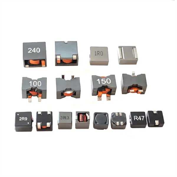
Inductive Components
#inductive #charging #components <br>[a]https%3A%2F%2Fwww.magnetic-cube.com%2Fproducts%2F[/a] <br> <br>Inductive components, such as inductors and transformers, are essential in electronics, aiding in energy storage, signal processing, and filtering. These electric circuit components types store energy in a magnetic field, playing a pivotal role in the functionality and efficiency of various electronic systems. <br> <br>Specific Information for Inductive Components <br>Inductive components are passive Electronic component China that use the principle of electromagnetic induction to store and transfer energy. They are widely used in various electronic circuits and systems. Here is some specific information about electronic component wholesale: <br> <br>Types of Inductive Components: The most common types of inductive components include inductors, transformers, and chokes. <br> <br>Inductors: Inductors are passive electronic components that store energy in a magnetic field when an electric current flows through them. They are typically made of a coil of wire wound around a core material, such as iron or ferrite. Custom inductors are used in various applications, including filtering, energy storage, and impedance matching. <br> <br>Transformers: Transformers are inductive components that transfer electrical energy between two or more circuits through electromagnetic induction. They consist of two or more coils of wire wound around a common core material. Transformers are used to step up or step down voltage levels, isolate circuits, and match impedance. <br> <br>Chokes: Chokes, also known as inductor filters or reactors, are inductive components used to block or filter out high-frequency noise or ripple currents in electronic circuits. They are designed to have a high inductance value and are often used in power supplies and audio circuits. <br> <br>Inductance: Inductance is a property of passive components in electronics that determines their ability to store energy in a magnetic field. It is measured in henries (H) and depends on factors such as the number of turns in the coil, the core material, and the physical dimensions of the component. <br> <br>Core Materials: Inductive components can have different core materials, such as iron, ferrite, powdered iron, or air. The choice of magnetic core material depends on factors such as the desired inductance value, frequency range, and power handling capability. <br> <br>Inductive Reactance: passive electrical components exhibit a property called inductive reactance, which is the opposition to the flow of alternating current (AC) due to the inductance. Inductive reactance is directly proportional to the frequency of the AC signal and the inductance value. <br> <br>Quality Factor (Q): The quality factor is a measure of the efficiency of an inductive component. It represents the ratio of the reactive power stored in the component to the power dissipated as heat. A higher quality factor indicates a more efficient component. <br> <br>Saturation: Inductive components can experience saturation when the magnetic field strength reaches a maximum value, causing a decrease in inductance. Saturation can occur when the current flowing through the component exceeds its rated value or when the magnetic field strength exceeds the core material’s saturation level. <br> <br>Applications: Inductive components are used in a wide range of fields, the inductor application includes power supplies, audio systems, telecommunications, motor control, RF circuits, and many more. <br> <br>It is important to consider these specific details when selecting and using inductive components in electronic circuits to ensure proper functionality and performance. <br> <br>For more information about electronic component types and buy inductive transformers, please feel free to contact us! <br> <br>There are many electronic component manufacturers, but we are one of the best choices for you. <br> <br>If you are looking for a reliable electronic component company, don't hesitate to contact us!
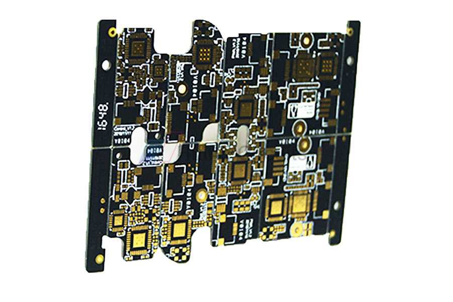
Heavy Copper PCB Manufacturer
Heavy Copper PCB, pcb fabrication up to 12oz, large current, pcb circuit fabrication base material is FR4/Teflon/Ceramic, pcb fabrication used in high-power power supply and motor circuits products. HUIHE CIRCUITS is one of the heavy copper PCB manufacturers, we have passed ISO9001/ISO13485/IATF16949/UL/RoHS/REACH certification.If you want to know more about thick copper pcb, heavy copper pcb, please contact HUIHE Circuits heavy copper pcb board manufacturer. <br> <br>Heavy Copper PCB List <br>2 Layer ENIG Heavy Copper PCB circuit manufacturer <br> <br>4 Layer ENIG Heavy Copper PCB <br> <br>6 Layer ENIG Heavy Copper PCB supplier <br> <br>6 Layer ENIG Heavy Copper PCB manufacturing <br> <br>6 Layer ENIG Heavy Copper PCB Fabrication Service <br> <br>6 Layer ENIG Heavy Copper PCB <br> <br>8 Layer ENIG Heavy Copper PCB <br> <br>8 Layer ENIG Impedance Control Heavy Copper PCB <br> <br>2 Layer ENIG Heavy Copper PCB <br> <br>The Heavy Copper PCB Plating Process Must Achieve The Following Aspects: <br>1. HUIHE Circuits heavy copper pcb manufacturer adds a certain value according to the area value calculated by the computer and the empirical constant accumulated in the actual production to ensure the integrity of the plating layer in the hole. <br>2. When the heavy copper PCB is electroplated for 5 minutes, take out the substrate and observe whether the copper layer on the surface and the inner wall of the hole is intact. It is better that all the holes have a metallic luster. <br>3. A certain distance must be maintained between the substrate and the substrate. <br>4. When the heavy copper PCB reaches the required electroplating time, a certain amount of current must be maintained during the removal of the substrate to ensure that the surface of the substrate and the hole will not be blackened or darkened. <br>5. HUIHE Circuits heavy copper pcb manufacturer according to the mechanical processing floppy disk for trial processing, the first part pre-inspection is carried out, and all the workpieces are processed after meeting the technological requirements. <br>Heavy Copper PCB Manufacturer Quality Control <br>1. HUIHE Circuits heavy copper PCB manufacturer Strictly implements the first article inspection system to ensure that the product size meets the design requirements. <br>2. According to the raw materials of different types of pcb boards, reasonably select the milling process parameters. <br>3. When fixing the position of the circuit board, HUIHE Circuits heavy copper PCB manufacturer carefully clamps it so as not to damage the solder layer and solder mask on the surface of the circuit board. <br>4. To ensure the consistency of the substrate dimensions, HUIHE Circuits heavy copper PCB manufacturer must be strictly controlled the position accuracy . <br>5. When disassembling and assembling, HUIHE Circuits heavy copper PCB manufacturer pays special attention to the barrier layer of the substrate and pad paper to avoid damage to the coating layer on the surface of the circuit board. <br>Applications Of Heavy Copper PCB <br>Heavy copper PCBs shine in applications that demand high power and efficient heat management. Here are some key areas where they are widely used: <br> <br>Power Electronics: This is a major domain for heavy copper PCBs. They are ideal for power supplies, motor controllers, and other high-current devices. Their ability to handle large currents and dissipate heat effectively makes them perfect for these applications. <br>Industrial Automation: Industrial equipment often involves high-power motors, drives, and converters. Heavy copper PCBs ensure smooth operation by handling substantial currents and dissipating the generated heat. <br>Automotive Industry: Modern vehicles use increasingly complex electronic systems, including power converters and inverters. Heavy copper PCBs provide the necessary current capacity and thermal management for these applications. <br>Aerospace and Defense: These sectors demand reliable and high-performance electronics. Heavy copper PCBs meet these needs with their superior current handling and heat dissipation. <br>Other Applications: They can also be found in welding equipment, power distribution units, power line monitors, torque controls, overload relays, and protection relays. <br>Overall, anywhere you need a PCB to handle significant power and manage the resulting heat, heavy copper PCBs are a strong choice. <br>#heavy#copper#pcb#manufacturers <br>[a]https%3A%2F%2Fwww.hhcircuits.com%2Fheavy-copper-pcb[/a]
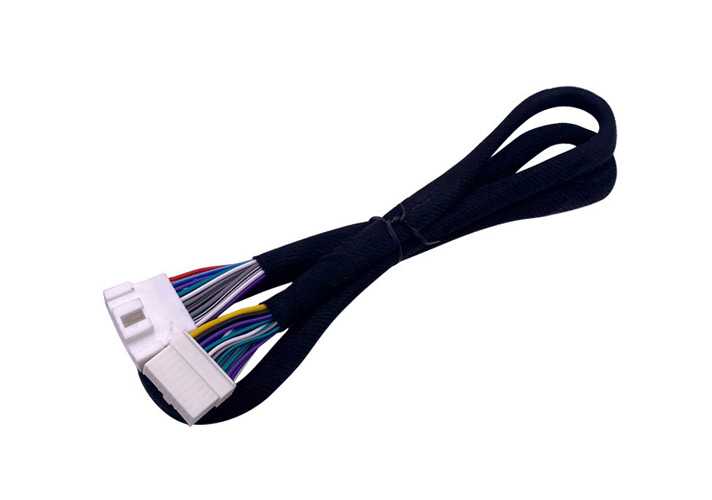
Auto Parts Wiring Harness
[a]https%3A%2F%2Fwww.holly-electronics.com%2Fproducts%2Fauto-parts-wiring-harness%2F[/a] <br>#cable #assemblies #factory <br>Auto Parts Wiring Harness <br>Holly electronic car auto parts wiring harness is a car DSP power amplifier refit special car wiring harness, 1/4 meter non-destructive installation extension tail wire, pure copper non-destructive wiring harness. <br> <br>Auto Parts Wiring Harness Features <br>01. <br>Connector <br>Special car connector, non-destructive docking. <br> <br>02. <br>Material <br>Made of high quality PVC flame retardant material, this type of audio and video wire is safe and stable. <br> <br>03. <br>Transmission <br>Pure copper tinned copper wire transmission signal, fidelity sound quality. <br> <br>04. <br>Coverage <br>Universal connector model, high coverage. <br> <br>Specifications of Auto Parts Wiring Harness <br>Product name: Car audio wire CD tail wire car music wire harness <br> <br>Connector: Delphi brand products. <br> <br>Wire: UL certified 16AWG wire, copper wire high precision, oxygen free Copper: low resistance, good electrical conductivity. <br> <br>PVC cover: good wear resistance, oil resistance and elasticity. <br> <br>If you want to know more kinds of universal wiring harness for car stereos, please visit our website. <br> <br>As a cable assemblies factory, we can provide kinds of custom fiber optic assemblies for sale, if you are interested, please leave us a message.
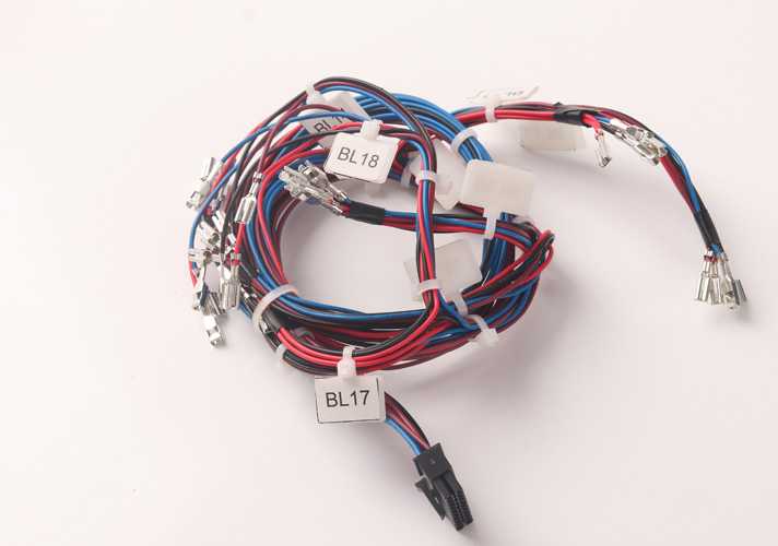
Vending Machine Wiring Harness
[a]https%3A%2F%2Fwww.holly-electronics.com%2Fproducts%2Fautomat-wiring-harness%2F[/a] <br>#custom #hybrid #cables <br>Vending Machine Wiring Harness <br>Vending machine wiring harness, also known as unmanned vending machine oem wiring harness, delivers customers' needs for beverages, food, fresh vegetables and personal items to customers through the vending wire produced by Holly Electronics. The vending wire is very convenient for people to buy demand, but also greatly reduces the cost of business on the site, personnel, and time. <br> <br>Vending Machine Wiring Harness Features <br>01. <br>Product Test <br>Products through UL VW-1 vertical fire resistance test, green environmental protection, Rohs test report. <br> <br>02. <br>Custom Electronic Harness <br>Engineers with more than 20 years of experience in wire harness & cable assembly manufacturing analyze power electronics products and design custom electronic harness. <br> <br>03. <br>Provide Reliable Vending Machine Harness <br>Provide reliable performance of the vending machine wiring harness, connector using TE, MOLEX brand products, to ensure the accuracy of signal transmission. <br> <br>04. <br>Ul, VDE Certified Products <br>All cables using UL, VDE certification products, wire using pure copper tin material wire core, strong signal transmission, stable performance. <br> <br>05. <br>Features <br>Flame retardant, high temperature resistant, waterproof and moistureproof. <br> <br>Applications of Vending Machine Wiring Harness <br> <br>Molex5557 connector series, classic and reliable; <br> <br>TE187 connection terminal, stable conductive connection; <br> <br>Ul1007-20awg tin plated wire, economical. <br> <br>If you want to know more kinds of custom hybrid cables, please visit our website.
Multilayer PCB Manufacturing up to 38 Layers
Multilayer PCB Manufacturing up to 38 Layers <br>Multilayer PCB Manufacturing up to 38 layers <br> <br> <br> <br>Rigid Circuit Board Manufacturer & Assembly – One stop service PCB rigid Circuit Board is an important electronic component, support for electronic components, and a carrier for electrical connection of electronic components. Read on to learn more about multilayer PCBs, their uses and advantages in the world of modern electronics. <br> <br> <br> <br>A Multilayer Printed Circuit Board, or Multilayer PCB, is a complex circuit board composed of multiple layers of conductive material and insulating material (usually fiberglass and epoxy resin) sandwiched together. Multilayer PCB or multilayer printed circuit boards are circuit boards composed of two or more conductive layers (copper layers). The copper layer is pressed together by the resin layer (prepreg). Each layer has a conductive path or copper trace, and each layer is connected to one another through pads and vias, which act as electrical conduits. This construction allows for more complex and dense circuitry to be designed, with greater functionality and reliability compared to single- or double-sided PCBs. Multilayer PCBs are commonly used in electronic devices such as computers, smartphones, and advanced medical equipment. <br> <br> <br> <br>Multilayer PCB Prototype manufacturing <br> <br>What is Multilayer Printed Circuit Board? <br> <br> <br> <br>A Multilayer Printed Circuit Board (PCB) is a type of PCB that consists of several layers of conductive material and insulating material sandwiched together. The board is made by laminating together multiple thin layers of fiberglass or other insulating materials with copper foil. <br> <br>An integrated circuit is placed on the board, and the copper traces connected to the circuit are etched onto the inner layers of the board. The inner layers are then sandwiched together with the outer layers, forming a multilayer structure. <br> <br>Multilayer PCBs are used in high-end electronic products, such as advanced computers and mobile phones, where a high degree of density is required, and the manufacturing process is complex. They provide many benefits, including reduced size, increased reliability, and improved performance. <br> <br>Multilayer PCBs are cost-effective because they reduce the total number of components needed and improve product reliability, thus reducing the need for frequent repair services or replacement. The design flexibility of these boards also allows for more efficient use of space and improved signal routing, which aids in the performance of the product. <br> <br> <br> <br>Multilayer Printed Circuit Board stack up <br> <br> <br> <br>So what’s Multilayer PCB Benefits / Advantages? <br> <br> <br> <br>1. Increased Design Flexibility: Multilayer PCBs allow for more design flexibility and greater circuit density. With multiple layers, engineers have more space to incorporate more components and features, such as impedance control, shielding, and power planes, within the same board area. <br> <br> <br> <br>2. Increased Reliability: Multilayer PCBs are more reliable than single sided PCBs, as they are less prone to issues such as signal interference, voltage drops, and thermal stress. This is because they have a higher number of conductive layers, which allows for better shielding and more stable power distribution. <br> <br> <br> <br>3. Higher Component Density: Multilayer PCBs can accommodate a higher density of components in a smaller space while preventing signal interference. This results in a more compact and efficient design, saving manufacturers money on materials and production. <br> <br> <br> <br>4. Improved Signal Integrity: With a multilayer construction, PCBs can have better signal integrity, which means less noise and less chance of signal interference. The numerous grounds and power planes help to suppress electromagnetic interference, resulting in better connection quality. <br> <br> <br> <br>5. Better Thermal Management: Multilayer PCBs have better thermal conductivity, which reduces hot spots and improves heat dissipation. The extra layers also help to keep the heat from spreading across the board, which is important for high-power applications. <br> <br> <br> <br>6. Cost-Effective: While the initial cost of multilayer PCBs may be higher than single or double-sided PCBs, the benefits in terms of increased density, reliability, and design flexibility can mean overall cost savings in the long run. Additionally, as manufacturing techniques have evolved, the cost of producing multilayer PCBs has become more competitive. <br> <br> <br> <br>In summary, the benefits of multilayer PCBs include increased design flexibility, reliability, component density, and thermal management. They also offer improved signal integrity and can be cost-effective in the long run. These advantages make them suitable for complex electronic devices where high performance, reliability, and space-saving are required. <br> <br> <br> <br> <br> <br>-While Multilayer Printed Circuit Boards (PCBs) offer many benefits over single- or double sided PCBs, there are also some potential drawbacks to consider: <br> <br> <br> <br>1. Complexity: The multilayer PCBs are far more complex than their single-layered or double-layered counterparts. As the number of layers increases, so does complexity. This means that design and manufacturing is more challenging, which can lead to a higher cost of production. <br> <br> <br> <br>2. Cost: Multilayer PCBs are generally more expensive than single or double-layered PCBs due to their complexity. The cost of producing multilayer PCBs can increase exponentially, and the cost of manufacturing is highly dependent on the number of layers in the board, the board size, and overall complexity. <br> <br> <br> <br>3. Signal Integrity: Multilayer boards pose a higher risk of signal integrity issues due to the higher number of components and traces present in each layer. Signal interference, crosstalk, and noise can occur if proper precautions are not taken in the design process. It is therefore essential that the designer takes signal integrity into account while designing the board. <br> <br> <br> <br>4. Manufacturing Challenges: The process of cutting, etching, drilling, and laminating the multiple layers of a PCB requires highly precise equipment, which can add to the cost of manufacturing. Moreover, misalignment of layers and flaw in lamination can lead to defects that can potentially cause the PCB to stop functioning correctly. <br> <br> <br> <br>5. Environmental Impact: Multilayer PCBs contribute to electronic waste, which is a significant concern for the environment. The process of manufacturing multilayer PCBs consumes a considerable amount of energy, and the resulting waste can be toxic and difficult to recycle. <br> <br> <br> <br>Overall, Multilayer PCBs offer many advantages over single or double-sided PCBs. However, there are several issues that need to be considered during the design and manufacturing process, to achieve optimal performance. To solve your problems, here HITECH Circuits provide solutions for you. <br> <br> <br> <br>Multilayer Printed Circuit Board <br> <br> <br> <br>-Multilayer Printed Circuit Boards (PCBs) are used in a variety of applications where high performance and reliability are critical. Here are a few of the most common applications: <br> <br> <br> <br>1. Communications: Multilayer PCBs are widely used in the telecommunications industry for various applications such as cell phone base stations, satellite communications systems, and other communication devices that require high-speed data transfer rates and minimal signal loss. <br> <br> <br> <br>2. Computers: Multilayer PCBs are extensively used in computer motherboards, laptops, and other computing systems where high performance, reliability, and miniaturization are of utmost importance. <br> <br> <br> <br>3. Medical Equipment: Multilayer PCBs are a key component in many medical devices, such as imaging equipment, patient monitoring systems, and surgical instruments, where high reliability and stability are required. <br> <br> <br> <br>4. Automotive: The automotive industry uses Multilayer PCBs for applications such as engine control units, airbag systems, and lighting control systems, where reliability, durability, and efficient operation are essential. <br> <br> <br> <br>5. Aerospace and Defense: Multilayer PCBs find extensive use in aerospace and defense applications, such as missiles, satellites, and other spacecraft, where superior performance and reliability are required in extreme conditions. <br> <br> <br> <br>Overall, Multilayer PCBs are used in a wide variety of applications where increased functionality, reliability, and performance are required. With advances in technology, the use of multilayer PCBs is expected to continue to grow in the future.
Best Flexible PCB Manufacturing
What is Flex PCB? <br> <br> <br> <br>Flexible printed circuits, also known as flex circuits, are sometimes regarded as a printed circuit board (PCB) that can bend, when in reality there are significant differences between PCB’s and flex circuits when it comes to design, fabrication and functionality. One common mistake that designers make is to design a flexible circuit using the same rules as a PCB. Flex PCB require a unique set-up and have their own set of design rules that the Hitechpcb team has termed “flex-izing” and have worked hard to perfect over the last many years. <br> <br> <br> <br>Flexible PCB, which also called Flex PCB, Flexible circuit board or flex circuit, it consists of PI base material, adhesive layer, copper layer, coverlay and sometimes with stiffeners. Flexible PCBs are now being used widely to replace traditional FR4 PCB in various different applications due to the benefits from flex PCB specially. Although more expensive than a normal rigid PCB, the right design in the right application could save weight and time in assembly, coupled with the reliability which makes flexible circuit board a worthwhile consideration. <br> <br> <br> <br>A flexible printed circuit consists of a metallic layer of traces, usually copper, bonded to a dielectric layer, usually polyimide. Thickness of the metal layer can be very thin (<.0001″) to very thick (> .010″) and the dielectric thickness can vary from .0005″ to .010″. Often an adhesive is used to bond the metal to the substrate, but other types of bonding such as vapor deposition can be used to attach the metal. <br> <br> <br> <br>flexible PCB <br> <br>How to calculate your flex pcb bend radius? <br> <br> <br> <br>Because copper tends to readily oxidize, the exposed surfaces are often covered with a protective layer, gold or solder are the two most common materials because of their conductivity and environmental durability. For non-contact areas a dielectric material is used to protect the circuitry from oxidation or electrical shorting. <br> <br> <br> <br>The number of material combinations that could go into a flexible printed circuit are nearly endless; current, capacitance, chemical and mechanical resistance, temperature extremes and type of flexing are just some of the criteria that impacts the material selections that best meet the functional needs. An experienced Hitechpcb design engineer takes the critical requirements into consideration when designing a circuit to meet your needs. <br> <br> <br> <br>Flexible printed circuit boards (FPC) has become a common component of electronic products due to its lightness and flexibility performance. It is widely used in smart terminal, wearable electronics, consumer, automotive, industrial and medical fields. The miniaturization and integrated function of electronics product development is driving FPC to fine line and multilayer design. <br> <br> <br> <br>What is Multilayer flex PCB? <br> <br>This type of flexible printed wiring boards are multilayered (with three or more conductor layers) and require plated-through holes. We could use through vias, buried vias and blind vias. <br> <br> <br> <br>A multi layer flex circuit combine several single-sided or double-sided circuits with complex interconnections, shielding and/or surface mounted technologies in a multi layer design. The multi layers may or may not be continuously laminated together throughout the production process. If your design needs require maximum flexibility, continuous lamination may not be appropriate. Multi layer circuits are an effective solution when confronted with design challenges such as: unavoidable crossovers, specific impedance requirements, elimination of crosstalk, additional shielding and high component density. You can also link here to learn more about flex pcb bending radius. <br> <br> <br> <br>Benefits to Flex PCB including: <br> <br>Assembly Error Reduction <br> <br>Decreased Assembly Time and Costs <br> <br>Design Freedom <br> <br>Flexibility during Installation <br> <br>High Density Applications <br> <br>Improved Airflow <br> <br>Increased Heat Dissipation <br> <br>Increased System Reliability <br> <br>Point-to-Point Wire Replacement <br> <br>Reliability and Durability <br> <br>Repeatable Routings <br> <br>Simplified Circuit Geometry <br> <br>Package Size and Weight Reduction <br> <br>Flex PCB Static Application <br> <br>An application where flexible circuits are flexed only to install the circuit and fit it into its application (also known as flex-to-fit or flex-to-install). A static application will typically be made using the less expensive Electro Deposited (ED) copper. <br> <br> <br> <br> <br> <br>Flex PCB Dynamic Flexing Applications <br> <br>A situation where the flexible circuit itself is dynamically (repeatedly) flexed during the actual use of the final product. Common examples include flip-type cell phones, laptops, printer heads and robotic arms. A dynamic application will require the use of Rolled Annealed (RA) copper. <br> <br> <br> <br>High Density Flex PCB Applications <br> <br>Flexible circuits allow for minutely narrow lines giving way to high density device population. Denser device populations and lighter conductors can be designed into a product, freeing space for additional product features. <br> <br> <br> <br>With a large number of investments on the facilities of flexible printed circuit board and continuously innovating the flexible circuit board manufacturing technology, Hitech Circuits is able to manufacture flexible PCBs with a great variety of technologies, from simple single sided flex PCB, double sided flex PCB to complex multilayer flexible PCB, Rigid flex pcb and support prototype FPC with laser cutting & flying probe test to mass production with toolings. <br> <br> <br> <br>Multilayer flex PCB bookbinding <br> <br>Circuit bookbinding is one of the best practices employed by Hitechpcb engineers for creating stacked PCBs. For flex PCBs, we offered a 12 layer flex PCB board with bookbinding. An additional small length is added to the circuit, making it move in an outward direction from the bend radius. There are copper traces placed at right angles to the bend. This helps restrict the circuit bend in one direction. <br> <br> <br> <br>The length to be added depends on total number of layers in the PCB, as well as the tightness of the bend. The advantage of circuit bookbinding is that it removes a great amount of tension from the various circuit layers during the bending process. The method also helps prevent buckling of the circuits at the exact bend radius. <br> <br> <br> <br>The bookbinded PCBs can easily meet the tight tolerance requirements in comparison to bonded PCBs. This is why this 12 layer flex PCB is a perfect choice for applications where stricter tolerances are required. Its polyamide construction delivers immense strength and flexibility. This flexi PCB can easily perform 180° bends. Also, the construction helps prevent buckling of inner layers, which often occurs in a long term use. This flexibility also helps reduce stress on the internal components. This 12 layer flex PCB board has better shelf life than a 12 layer bonded circuit board. The immersion gold plating offers low contact resistance, good wetting, as well as excellent shelf life. We can provide the 12 layer flex PCB board with book binding in width 4/4 mil, with minimum finish thickness 0.15 mm flex and maximum 1.6 mm. <br> <br> <br> <br>Advantages of Flexible PCB <br> <br> <br> <br>Flexible PCB technology often has a wide range of possibilities for different designs and products. <br> <br>The flexible feature is among the best attributes of the cables, wires, connectors and even PCBs. <br> <br>Some of the advantages of using the flexible circuit include: <br> <br> <br> <br>Reduces the overall weight and size. <br> <br>A flex circuit can reduce the weight of a device by up to 70%. <br> <br>Improves the packaging of electronics <br> <br>It gives you the ability to solve interconnect and packaging issues as it can bend, form and move. <br> <br>Interconnect solution as it reduces the amount of interconnects such as cables, wires, pcbs and connectors. <br> <br>Conformability as the slender nature of the material allows for making of 3D packages <br> <br>Electrical integration – You can easily come up with custom solutions basing your design on a plethora of choices of materials. Apart from that, you have the freedom to choose from the myriad of designs and plating procedures. <br> <br>Heat dissipation ability or power – The polyimide dielectric has the ability to withstand very high temperatures. You can, therefore, use it for high power applications. <br> <br>Electrical and mechanical repeatability <br> <br>Cost saving as you can save up to 30% of the total cost of hand wiring and other assembly processes. <br> <br>You can also save on space by almost 30% <br> <br>It is more reliable as it does not have any wiring errors <br> <br>Despite the numerous advantages, the flexible PCB also has its disadvantages. <br> <br>Let’s have a look. <br> <br> <br> <br>Disadvantages of Flexible PCB <br> <br>Every electronic solution must have certain demerits. <br> <br>Some of the disadvantages include: <br> <br>Flexible PCB <br> <br>A higher initial cost – Since the flex circuit is often custom for particular electronics. The initial cost of designing, photographic plate and layout is very high. This limits you to using it on large quantities to save on cost. <br> <br>Flexible circuit repairs and changes are very difficult – The initial process is not just expensive but difficult to come up with. Once you have the base map, it becomes difficult to make any more changes. Removing and replacing the covering film for repair is also extremely difficult. <br> <br>It is often small in size – The batch process of making the flexible circuits often limits the size of the flexible circuit. The production equipment limits you from making wider and longer sizes. <br> <br>Easy to damage – Improper personal operations can easily damage the flexible circuits. Rework and soldering will require the expertise of a technician. <br> <br>The process of assembly is also very difficult. <br> <br>Do not let the disadvantages kill your spirits. <br> <br> <br> <br>Why Not Make All Circuit Boards Flexible? <br> <br> <br> <br>Flexible circuit boards are certainly useful, but they are not going to replace rigid circuit boards for all applications. Cost efficiency is the main obstacle to implementing an exclusively flexible circuit board design in a consumer product. Rigid circuit boards are less expensive to manufacture and install in a typical automated high-volume fabricating facility. <br> <br> <br> <br>Typically, the ideal solution for an innovative product is one that incorporates flexible circuitry when necessary and employs solid, reliable rigid circuit boards where possible to keep manufacturing and assembly costs down. <br> <br> <br> <br>Some manufacturers even use hybrid rigid-flex printed circuit boards expressly for this purpose. This is common in laptop computers and medical devices, where rigid circuit boards can be connected to one other using ribbon-like flexible circuits. These boards can be compounded and designed to meet any number of engineering needs by focusing on the respective strengths of each circuit board base technology. <br> <br> <br> <br>Hitech Circuits creates both flexible and printed circuit boards for product manufacturers. Enjoy a consultation with one of our sales reps to find out if your product prototype design is best served by flexible or rigid circuit board types. <br> <br> <br> <br>What is Flexible PCB and Its Production Process? <br> <br> <br> <br>Flexible PCB (Flexible Printed Circuit, FPC) is very popular with excellent characteristics such as low weight and thin thickness, etc. It is also can be folded freely. Flexible PCB mainly relies on manual visual inspection with high cost and low efficiency. With the rapid development of the electronics industry, the design of printed circuit board has become more and more high -precision and high- density, traditional manual testing methods can no longer meet production needs. FPC defect automation testing has become an inevitable trend of industrial development. <br> <br>Flexible printed circuit (FPC) is a technology developed by theUnited Statesto develop aerospace rocket technology in the 1970s. It is high reliability, excellent deflection made by polyester film or polyimide as a substrate material. A flexible circuit is formed by embedding a circuit design in a thin, flexible plastic sheet that is flexible, allowing a large number of precision components to be stacked in a narrow and limited space. This circuit can be bent and folded at will. Flexible has the characteristics like light weight, small size, good heat dissipation, easy installation, etc, it breaks through the traditional interconnection technology in the structure of the flexible circuit, the material is composed of insulating film conductor and adhesive <br> <br> <br> <br>Flexible PCB includes single sided FPC, double sided FPC and multilayer FPC, etc. Single FPC has chemically etched conductive pattern layer, the conductive pattern layer on the surface of the flexible insulating substrate is calendered copper foil. The insulating substrate may be polyimide, polyethylene terephthalate, arylamide fiber ester and polyvinyl chloride. The double sided FPC on both sides of the insulating base has a conductive graphics made of etching, which increases the wiring density of the unit area. Metal hole connects the graphic connection on both sides of the insulation material to form a conductive pathway to meet the flexible design and function. The covering film can protect the single, double -sided wire and indicate the position of the component placed. According to demand, metal holes and coverage layers are optional. This type of Flexible PCB has fewer applications. Multi -layer flexible PCB is to press the single-sided or double-sided flexible circuit layer of 3 or more layers together. The metal hole is formed by drilling and electroplating, and conductive channels are formed among different layers. In this way, there is no need to use a complex welding process. Multi-layer circuits have huge functional differences in higher reliability, better thermal conductivity and more convenient assembly performance. <br> <br> <br> <br>At present, the production process of flexible PCB mainly includes looping, Sizing conductor, etching, routing of the conductors, ground planes, sizing of the holes, filleting, button plating, adhesive-backed films, screen-print liquid overcoats, photo imaginable liquid, film polymers and other processes. See the figure for the specific production process.
PNR Aviation Headset
#FNBV57 <br>A PNR (Passive Noise Reduction) aviation headset is a type of headset specifically designed for pilots and aviation professionals who require effective noise reduction during flights. PNR headsets utilize passive noise reduction techniques to minimize the impact of external noise on the user's hearing. With a specialized earcup for noise-proof insulation, it's worked by mechanically blocking sound waves from entering the ear. With NNR of 23dB, it's a perfect choice for aviators. <br> <br>What Is The Difference Between PNR And ANR Headset? <br>The terms pnr aviation headset and ANR refer to two different types of headsets commonly used in aviation and other noise-intensive environments. Here's a breakdown of their differences: <br>PNR (Passive Noise Reduction) Headset: <br>PNR headsets are equipped with passive noise reduction technology. They use physical materials and design features to block out external noise. The primary components of PNR headsets are ear cups with sound-absorbing foam padding and a tight seal around the ears. The foam absorbs and dampens the ambient noise, reducing its impact on the user's ears. <br>Pros of PNR headsets: <br> <br>Affordability: PNR headsets are more budget-friendly than ANR headsets. <br> <br>Durability: PNR headsets are known for their sturdy construction and ability to withstand wear and tear. <br> <br>Reliability: PNR headsets do not rely on batteries or electronics, making them less prone to power-related issues. <br> <br>Lower power consumption: PNR headsets don't require power, making them suitable for situations with limited power sources. <br> <br>Cons of PNR headsets: <br>They do not eliminate noise completely, as some sound can still leak in. <br>They are less effective in reducing low-frequency noise. <br>May cause ear discomfort during extended use due to the tight seal. <br>Relatively simple and less expensive compared to ANR headsets. <br> <br>No reliance on electronics or batteries, making them more reliable. <br> <br>Provide a consistent level of noise reduction across different frequencies. <br> <br>ANR (Active Noise Reduction) Headset: <br>ANR headsets utilize active noise cancellation technology. They incorporate microphones on the outside of the ear cups that detect ambient noise. The headset then generates an "anti-noise" signal that is precisely out of phase with the detected noise. When the anti-noise signal combines with the ambient noise, they cancel each other out, resulting in reduced noise levels reaching the user's ears. <br>Pros of ANR headsets: <br> <br>Effective noise cancellation: ANR headsets use active technology to cancel out external noise, providing a quieter listening experience. <br> <br>Enhanced comfort: ANR headsets are designed with ergonomic features and cushioning for a more comfortable fit during extended use. <br> <br>Customizable noise cancellation: ANR headsets often offer adjustable noise cancellation levels, allowing users to control the amount of noise reduction based on their preference and the surrounding environment. <br> <br>Improved audio clarity: By reducing background noise, ANR headsets enhance the clarity and intelligibility of audio communication and entertainment. <br> <br>Cons of ANR headsets: <br>ANR headsets are generally more expensive due to the added technology. <br> <br>They require batteries or power source to operate the active noise cancellation circuitry. <br> <br>Some ANR headsets may introduce slight audio artifacts or a faint "hissing" sound due to the cancellation process. <br> <br>Highly effective in reducing both low-frequency and high-frequency noise. <br> <br>Offer superior noise reduction compared to PNR headsets. <br> <br>Provide a more comfortable listening experience as they don't rely solely on physical pressure around the ears. <br> <br>In summary, PNR headsets use passive methods like foam padding and a tight seal to reduce noise, while ANR headsets employ active noise cancellation technology to actively counteract ambient noise. ANR headsets generally offer higher noise reduction capabilities, but they come at a higher cost and rely on batteries or power. The choice between PNR and ANR headsets depends on personal preference, budget, and the specific noise environment in which they will be used. <br> <br>Key Features of PNR Headsets <br>PNR (Passive Noise Reduction) headsets offer several key features that contribute to their effectiveness in reducing external noise. Here are some of the important features you can expect to find in a PNR headset: <br> <br>Ear Cups: PNR headsets typically have large ear cups that encompass the ears entirely. The ear cups are designed to provide a secure fit and create a seal around the ears, preventing external noise from entering. <br> <br>Sound-Absorbing Padding: The ear cups of PNR headsets are lined with sound-absorbing padding or foam. This padding helps absorb and dampen ambient noise, reducing its impact on the user's ears. <br> <br>Sealing: PNR headsets employ a sealing mechanism to enhance noise reduction. The ear cups are designed to fit snugly around the ears, effectively blocking out external sounds and creating a quieter listening environment. <br> <br>Adjustable Headband: PNR headsets typically feature an adjustable headband that allows users to customize the fit according to their head size and comfort preferences. The headband ensures a secure and comfortable fit during extended use. <br> <br>Boom Microphone: Many PNR headsets come with a boom microphone attached to one of the ear cups. The boom microphone allows for clear voice transmission and communication with air traffic control or other personnel. <br> <br>Volume Control: PNR headsets often have built-in volume control options. These controls enable users to adjust the audio output to their desired level, ensuring clear communication and comfortable listening. <br> <br>Durability: PNR headsets are designed to withstand the demanding conditions of aviation environments. They are typically constructed using durable materials that can withstand frequent use, rough handling, and exposure to various elements. <br> <br>Weight and Comfort: PNR headsets aim to provide a balance between noise reduction and comfort. They are designed to be lightweight and ergonomic, minimizing discomfort during prolonged use. <br> <br>Compatibility: PNR headsets are compatible with standard aviation audio systems and intercom systems commonly used in aircraft. <br> <br>It's important to note that the specific features and design may vary among different models and brands of PNR headsets. It's recommended to review the specifications and features of a particular headset before making a purchase to ensure it meets your specific needs and preferences. <br> <br>Ray talk, as an excellent call center head set manufacturer, offers a wide range of call center head set for you to choose from. <br> <br> <br> <br>[a]https%3A%2F%2Fwww.raytalkcomms.com%2Fproducts%2Fpnr-aviation-headset%2F[/a]
3.0mm Connector
Connectors are crucial components in electronic devices, ensuring seamless power and data transmission. The 3.0mm connector is widely used in various applications due to its robust design and reliable performance. This connector size is ideal for power supply connections in devices that require a stable and strong connection. Its larger size compared to other connectors allows it to handle higher currents, making it suitable for power-intensive applications such as industrial equipment and large household appliances. The 3.0mm connector's durability and ability to maintain a secure connection even in demanding environments make it a popular choice for engineers. <br>In contrast, the 0.8mm connector is known for its compact size, making it perfect for applications where space is at a premium. This type of connector is commonly found in mobile phones, tablets, and other compact electronic devices. Despite its small size, the 0.8mm connector offers reliable performance and ensures stable connections. Its design allows for high-density configurations, which is crucial in modern electronic devices that are becoming increasingly compact. The precision engineering behind these connectors ensures that they can handle the rigorous demands of portable electronics, including frequent plugging and unplugging. <br>The 1.25mm connector strikes a balance between the 3.0mm and 0.8mm connectors, offering a medium size that provides both versatility and reliability. This connector is often used in applications like computer peripherals and small household electronics. The 1.25mm connector is favored for its ability to provide stable connections while maintaining a relatively small footprint. Its versatility makes it suitable for a wide range of applications, from data transmission in computer networks to connecting components within various electronic devices. The 1.25mm connector's blend of size, reliability, and performance ensures it remains a staple in many electronic designs.
LOW PRESSURE Molding
#insert #molding <br>LOW PRESSURE Molding <br>As the name suggests, low pressure molding, low pressure forming is a process that injects materials into a mold with very low injection pressure and solidifies quickly. <br> <br>Low pressure injection molding typically involves the use of an insert, rather than solely injecting a product. Molten plastic is then injected into the mold cavity at a low pressure. Once the plastic has cooled, the insert is fused with the plastic to form a cohesive plastic component. <br> <br>WHY CHOOSE <br>CN Low Pressure Molding <br>1. We offer comprehensive low pressure injection molding solutions that cover everything from design for manufacturing to DFM, mold design and fabrication, materials selection, equipment, and process parameter optimization. <br> <br>2. Possess a high-performance low pressure molding systems that can meet your product needs. <br> <br>3. Our company possesses a professional design team that provides technical support throughout the production process for you. <br> <br>4. Get certified with ISO 9001:2015 and IATF 16949:2016 to ensure the quality of your products. <br> <br>#APPLICATION <br>LOW PRESSURE MOLDING Application <br>Low pressure injection molding is distinguished from traditional injection molding by its lower injection pressure. This feature offers the advantage of reducing the likelihood of damaging the encapsulated parts. As a result, low pressure moulding processes find primary use in two distinct applications: <br> <br>1. In electronic and electrical industry: printed circuit boards, automotive electronic products, sensitive components, mobile phone batteries, cables, connectors, sensors, etc. <br> <br>2. In automotive industry: door guard plates, column guard plates and wrap frame guard plate covered with skin such as fabric, PVC fabric. <br> <br>Low Pressure Molding Application <br>#ADVANCED LOW PRESSURE MOLDING <br>HOW DOES <br>Low Pressure Molding Work? <br>How Does Low Pressure Molding Work? <br>Step 1 : Put the electronic parts into the predetermined mold cavity. <br> <br>Step 2 : Use low pressure to inject plastic, then apply low pressure molding using a machine for Overmolding. <br> <br>Step 3 : After cooling, remove the plastic parts manually and inspect them. <br> <br>#ADVANCED MANUFACTURING <br>THE DIFFERENCE BETWEEN Low Pressure Molding And LSR Molding <br>Low pressure molding (LPM) and injection molding are both popular manufacturing processes for creating plastic parts, but they have some key differences in terms of materials, processes, applications, and advantages. Here's a comparison: <br> <br>Material: <br> <br>LPM uses a limited range materials, like PO, PP, PA, and even epoxy and polyurethane.Injection molding primarily uses thermoplastic materials that can melt and re-solidify, such as PP, PE, ABS, and PS. <br> <br>Process: <br> <br>LPM utilizes moderate pressure (around 3.5-14 bar) to inject molten plastic into a mold cavity. Injection molding employs high pressure (150-3000 bar) to rapidly inject molten plastic into a closed mold cavity under high pressure, then cools and solidifies it. <br> <br>Applications: <br> <br>LPM is often used for simpler parts where high precision is not critical.Injection molding is best suited for complex, high-precision parts requiring tight tolerances and intricate details, like gears, housings, electronic components, and medical devices. <br> <br>Summary: <br> <br>LPM molds are generally less expensive than injection molding molds due to their simpler design and lower pressure requirements. <br> <br>LPM offers more flexibility in material selection, while injection molding offers better control over material properties. <br> <br>Both processes are capable of high throughput, but injection molding can achieve faster cycle times for complex parts. <br> <br>Surface finishes can be comparable for both methods, but injection molding offers a nicer and wider range of finishing options. <br> <br>Ultimately, the best choice between LPM and injection molding depends on your specific project requirements and priorities. <br> <br>#ADVANTAGES <br>EXPLAIN ADVANTAGES OF Low Pressure Molding <br>RELIABLE <br>The low pressure molding product offers effective defense against water, dust, chemicals, shock, vibration, and high temperatures, and superbly relieves pressure. <br> <br>QUICK <br>Simplify the production process, cut production time, increase productivity, reduce the rejection rate, and lower production costs. <br> <br>ECO-FRIENDLY <br>Choose materials that are eco-friendly, reduce the use of unnecessary materials, and minimize material waste. <br> <br>#LOW PRESSURE MOLDING MATERIALS <br>MATERIALS OPTION OF CN's Low Pressure Molding <br>Low pressure molding is a great method to protect sensitive components. The type of plastic used is crucial because it impacts the strength, durability, and thickness of the final product. Thus, it's essential to select the right materials for different application, as outlined below: <br> <br>1. For automotive electronic parts, It is advisable to utilize materials that can withstand high temperatures as the surrounding temperature can be quite elevated. <br> <br>2. For outdoor electronics, such as wearable devices, bicycle components, underwater devices, or sensors, it may be necessary to use materials with a higher viscosity. <br> <br>In CN, the most commonly used material for low-pressure molding is polyamide (PA). It is chosen because of its high mechanical properties and melting point. In particular, components produced from PA materials display exceptional durability against wear and tear, possess natural lubrication capabilities, and exhibit strong resistance to fatigue. <br> <br>Now tthe price of injection molding mold is reasonable, if you have needs, please contact us. <br> <br>[a]https%3A%2F%2Fwww.cnmouldplastic.com%2Flow-pressure-molding%2F[/a]
LSR Molding
#multi #injection #molding <br> <br>LSR Molding <br>Liquid Silicone Rubber(LSR) has been in high demand since its development in these days. That's hardly surprising given its physical properties and the variety of applications it may serve. LSR is long-lasting, flexible, stable, and versatile. Customers appreciate the dependability and quality that our company consistently provides, so it's no wonder that our influence in the LSR sector is expanding as well. <br> <br>Injection moulding of liquid silicone rubber is a process that involves mixing two-part Liquid Silicone Rubber material, then curing it thermally in a mold using a platinum catalyst to produce silicone rubber parts and products. <br> <br>Liquid Silicone Rubber Molding is quite similar to the traditional process of plastic injection molding. However, the primary distinction between the two methods is that the conveying system for materials is cooled while the mold is heated. <br> <br>CN: The Perfecting LSR Process <br>STEP1 <br>Put the base-forming silicone and the platinum catalyst parts of the Liquid Silicone Rubber compounds A & B into the pumping system using the supply drums. Additionally, there is a separate container for the additives and color pigments. <br> <br>STEP2 <br>Mix the two Liquid Silicone Rubber, base-forming silicone and platinum catalyst by using the metering unit. Make sure that the two Liquid Silicone Rubber are kept at a consistent ratio of 1:1 while being transported simultaneously. <br> <br>STEP3 <br>Set up and start machine, Inject these mixed compounds into the mold cavity via nozzle and cold runner system. <br> <br>STEP4 <br>Once the silicone rubber products have undergone vulcanization and solidification, they can be removed from the mold either automatically or manually. <br> <br>STEP5 <br>The product will be post-processed and inspected. <br> <br>#APPLICATION <br>LSR MOLDING Application <br>Liquid Silicone Rubber is a material that extremely wide applications, suitable for numerous applications in various industries including medical, life sciences, automotive, consumer goods, and industrial products. <br> <br>Medical & Health: Medical tube, Endoscope components, Breathing face mask, Laryngeal mask; <br> <br>Automobile: Gasket, O-Ring, Seals, Optical coupling LED lens; <br> <br>Optics: Exterior and professional Lighting; <br> <br>Electronics: LED lens, protective cases, Watch bands, Silicone Lightning Cable; <br> <br>Consumer goods: Earphone, Earplugs, Eyeglass Nose Pads, safety goggles; <br> <br>Babies & Kids: Silicone baby bottles, Silicone pacifier, Silicone baby toothbrush. <br> <br>In short, there are numerous products that can be manufactured through the process of liquid silicone molding . <br> <br>WHY CHOOSE CN LSR Molding <br>EXTENSIVE EXPERIENCE <br>For almost 20 years, CN Mould & Plastic Limited has focused on making injection molds and doing injection molding. CN are fully knowledgeable about the LSR molding process and can handle problems that other companies might not be able to handle. <br> <br>HIGH EFFICIENCY <br>We are capable of creating prototypes for your parts within a short time frame. This speedy prototyping process enables you to swiftly enhance your parts and commence the production of components promptly. <br> <br>CUSTOMIZATION <br>Our team of engineers can assist you in selecting the appropriate type of LSR for your project, producing the products you require. We offer a complete range of services, including mold design, production, assembly, and coordination throughout the entire process. <br> <br>QUALIFICATIONS <br>CN has been certified in Quality Management by the International Organization for Standardization (SGS) according to the ISO 9001:2015 and IATF 16949:2016 disciplines. <br> <br>CRITICAL ADVANTAGES OF <br>LSR Molding <br>Advantages of LSR Molding <br>LSR's versatility and impressive properties make it a valuable material for a wide range of applications. From everyday gadgets to cutting-edge medical devices, LSR is shaping the future in many ways. <br> <br>Crystal Clear and Tough: LSR boasts excellent transparency, allowing intricate details to shine through. It's also tear-resistant, meaning it can handle wear and tear without breaking easily. It even resists turning yellow over time, keeping your products looking fresh. <br> <br>Temperature Hero: This material is truly extreme temperature resistant, functioning well even in extreme temperatures ranging from -60°C to 250°C. So, whether you're dealing with icy winters or scorching summers, LSR can handle it. <br> <br>Durable and Dependable: Strong, flexible, and stable, LSR offers long-lasting performance. It can even act as an insulator, preserving both electrical and thermal conductivity when needed. <br> <br>Automotive Applications: In the automotive world, LSR shines due to its heat resistance, ability to compress without losing shape, and excellent resistance to chemicals. It's commonly used in sensor covers, seals, and even interior components. <br> <br>Beyond Cars: LSR's chemical resistance and ability to withstand extreme temperatures make it popular in consumer electronics too. You'll find it in things like remote control buttons, phone cases, and even smartwatch bands. The growing popularity of wearable tech is expected to further boost the demand for LSR in this industry. <br> <br>Medical Marvel: Because LSR is highly inert, biocompatible, and hypoallergenic, it's safe for use in medical devices like prosthetics and even artificial organs. However, it's important to note that it can degrade in highly acidic environments. <br> <br>#ADVANCED LSR MOLDING <br>HOW DOES LSR Molding Work? <br>STEP1 <br>Put the base-forming silicone and the platinum catalyst parts of the Liquid Silicone Rubber compounds A & B into the pumping system using the supply drums. Additionally, there is a separate container for the additives and color pigments. <br> <br>STEP2 <br>Mix the two Liquid Silicone Rubber, base-forming silicone and platinum catalyst by using the metering unit. Make sure that the two Liquid Silicone Rubber are kept at a consistent ratio of 1:1 while being transported simultaneously. <br> <br>STEP3 <br>Set up and start machine, Inject these mixed compounds into the mold cavity via nozzle and cold runner system. <br> <br>STEP4 <br>Once the silicone rubber products have undergone vulcanization and solidification, they can be removed from the mold either automatically or manually. <br> <br>STEP5 <br>The product will be post-processed and inspected. <br> <br>#FAQS <br>FAQ OF Liquid Silicone Rubber Molding <br> <br>What is Liquid Silicone Rubber? <br> <br>Liquid Silicone Rubber is an organic silicone material that is transparent, non-toxic, heat-resistant, highly resilient and flexible once it has set. When it undergoes sulfurization, it exhibits low viscosity, quick curing, shear thinning, and a high coefficient of thermal expansion. <br> <br>Liquid Silicone Rubber is a two-component material that has high transparency, strength and tear resistance. It can be processed through liquid silicone injection molding processes. <br> <br>The Characteristics of LSR <br> <br>Biocompatibility: After extensive experiments, it has been found that LSR is highly compatible with human tissues and fluids. In contrast to other elastomers, LSR is less prone to bacterial growth and does not cause contamination or corrosion of other materials. <br> <br>Chemical Resistance: LSR can withstand water, oxidation, and certain chemical solutions like acids and bases. <br> <br>Temperature Resistance: Compared to other elastomers, LSR can tolerate a variety of high/low temperature restrictions. <br> <br>Mechanical Properties: The LSR material has great stretchability, strong resistance to tearing and pulling, and remarkable flexibility. Its hardness can range from 5 to 80 Shore A. <br> <br>Electrical Properties: LSR has great insulation properties and is a great choice for many electrical applications. Silicone can withstand both higher and lower temperatures compared to traditional insulation. <br> <br>Transparency and Pigmentation: LSR has a natural transparency that allows for the production of colorful and customizable molded products. <br> <br>Now tthe price of china injection molding mold is reasonable, if you have needs, please contact us. <br> <br>[a]https%3A%2F%2Fwww.cnmouldplastic.com%2Flsr-molding%2F[/a]
INSERT Molding
#injection #molding #exporter <br>INSERT Molding <br>Insert molding is a particular subset of injection molding used specifically to fuse many materials into one finished product. Therefore, the fundamental principle of custom insert molding is the same as that of injection molding. <br> <br>A pre-prepared insert is inserted in the mold by hand or by machine at the correct location, followed by the injection of molten plastic into the mold cavity. The insert is joined with the cooled and solidified plastic to create the final product once the mold is opened. With the help of this insert injection technique, the parts characteristics can be improved along with its overall stability. As a result, insert injection molding has been an increasingly common injection process in recent years. Typical example of insert molding applications is connector housing that combines machined metal pins with plastic. <br> <br>TYPES OF Insert Molding From CN <br>Stamped Parts Insert Molding <br>Angled Pins Insert Molding <br>POGO Pins Insert Molding <br>Magnet Insert Molding <br>PCB Insert Molding <br>Metal Insert Molding <br>Rubber Insert Molding <br>Silicone Insert Molding <br>Micro Insert Molding <br> <br>#ADVANCED MANUFACTURING <br>WHY CHOOSE CN Insert Molding <br>Extensive Experience <br>EXTENSIVE EXPERIENCE <br>Over 20 years, CN Mould & Plastic focus on making injection mold and develop an expertise of Elastomers. Tens of Millions of parts are shipped out each year to world-class customer such as HP, DELL, Apple. <br> <br>Development Advantage <br>DEVELOPMENT ADVANTAGE <br>Rich experience in injection molding and design flexibility for insert molding enable CN to quickly comprehend your need, cooperate with you to develop and improve products, and satisfy your customized requirements. <br> <br>Quality Assurance <br>QUALITY ASSURANCE <br>CN is certified by ISO 9001:2015 and ATF 16949:2016 discipline issued by the International Organization for Standardization (SGS) for Quality Management. Besides, we have a systematic program for handling complaints. <br> <br>Timely Delivery <br>TIMELY DELIVERY <br>Once we receive the customer's order, we will arrange the production as soon as possible. <br> <br>Our production philosophy is to achieve machine automation as much as possible, putting efficiency and quality in an important position to ensure timely delivery. <br> <br>#APPLICATION <br>INSERT MOLDING Application <br>If you need a high-quality, complex product, insert molding is a most efficient method that bonds effectively between plastic and inserts made from other materials. In particular, this process is ideally suited for the production of parts with extremely tiny tolerances and mass production. <br> <br>Because of this, insert molding technology has found increasing use in industries such as automotive, medicine, and consumer electronics in recent years. SIM card holders, connectors, charger housings, electrical wire connectors, and so on are all examples of common products made with insert molding. <br> <br>WHAT MATERIALS CAN BE USED IN INSERT MOLDING? <br>To precisely manufacture a plastic product via the injection molding process, a very tight tolerance is required. The molding process can fail even if there is only a tiny difference. Therefore, it is essential to know the shrinkage rate of the injecting material. Injecting materials for CN are usually chosen from nylon, PBT, and PPS. <br> <br>Materials for the insert need to be able to sustain the pressure of the injection molding process without being deformed; thus, metal, plastic, silicone, magnet, cable are all appropriate insert materials. In CN Mould, the insert molding process is widely applied to automotive accessories and electronic components, such as connector housing, charger housing, SIM card holders, cable components, etc. Therefore, metal is the most common material for inserts, for example, copper brass part, stamped part, angled pin, pogo pin. Of course, there are some special materials, like PCB. <br> <br>FAQ OF Insert Molding <br> <br>What's Insert Molding? <br> <br>Insert molding technology combines plastic with other different materials to form a single product. This may include combinations of plastic and metal, plastic and stamped insert, plastic and magnet, and so on. <br> <br>The Advantage of Insert Molding? <br> <br>1. Increase Design Flexibility. <br> <br>2. Reduces Assembly and Labor Costs. <br> <br>3. Increases Reliability. <br> <br>4. Reduces Size and Weight. <br> <br>When to Use Insert Molding? <br> <br>1. When using prefabricated substrates. <br> <br>2. If the substrate contains metal, cable, stamped part, or PCB. <br> <br>Note When Designing the Insert Molding Mold? <br> <br>1. Limiting tests for the part's shape and dimensional accuracy is crucial due to the inconsistent shrinkage rates of the materials during the insert molding process. <br> <br>2. Inserts can be deformed and shifted during the injecting process; therefore, it is necessary to fully take into account the shape of products and the position of inserts when designing the mold. <br> <br>3. Predicting gate location and molding cycle in advance is required. <br> <br>4. Confirming whether the insert requires pre-heating or drying treatment is necessary for ensuring both the quality of the finished product and the stability of the molding process. <br> <br>As one of insert molding manufacturers and insert molding suppliers, we will do our best to meet all the needs of customers. <br> <br>If you are looking for a reliable china injection mold factory, please choose us, and we will be your best partner. <br> <br> <br>[a]https%3A%2F%2Fwww.cnmouldplastic.com%2Finsert-molding%2F[/a]
MULTI-SHOT Molding
#injection #molding #cost <br>Multi Shot Molding <br>Different plastic materials and colors are used to create multi shot injection molding parts. In the process of injection molding, different materials must be tightly differentiated from one to another and cannot penetrate one another, like a Heart Rate Band. <br> <br>Different injection molding goods need to match different types of plastic materials in addition to materials with diverse hues, such as: <br> <br>1) The majority of the time, thermoplastic material and thermoplastic elastomer (such as TUE, TPU, etc.) are used to create products that combine soft and hard components. The product may have a rigid, corrosion-resistant matrix as a result of this combination, as well as a sealed anti-seismic or more pleasant feel. <br> <br>2) Items that incorporate Liquid Silicone Rubber (LSR). Since LSR has greater temperature resistance and mechanical qualities than thermoplastic elastomer, it is being used more frequently in multi material injection molding processes. <br> <br>#ADVANCED MANUFACTURING <br>WHY CHOOSE CN Multi-Shot Molding <br>1 <br>CN Mould & Plastic Limited launches its mold business in 2006 after more than 20 years of expertise in the production of injection molds. We are a multi shot injection molding factory and molder with expertise in Dual Shot Molding, Overmolding, and Insert Molding. Our skilled mold makers can offer high-quality, all-in-one service and injection mold creation. <br> <br>2 <br>Insert Molding and Overmolding are strong points of CN Mould & Plastic Limited. We frequently offer our customers product design recommendations as a way to improve Overmolding. CN Mould & Plastic Limited provides full-service contract manufacturing and has a design and development team for molding and tooling. In order to face each obstacle, we've been paying attention to what our clients desire and will keep developing our capabilities. <br> <br>3 <br>CN Mould & Plastic Limited has received certification for meeting the worldwide standards for the quality system in the medical industry, ISO 9001:2015 and IATF 16949:2016. CN Mould & Plastic Limited produces molds for a variety of sectors and provides services to the USA, Canada, and Europe. The largest tool is up to 1.3 meters in length. <br> <br>4 <br>With imported EDM and high-speed CNC precision process machines, CN Mould & Plastic Limited will check color, appearance and tolerance through quality control at every stage of the manufacturing process. We can assist you in creating any type of injection mold, even one with intricate structures. During the creation of injection molds, strict quality control is also utilized. <br> <br>MATERIALS OPTION OF <br>CN's Multi-Shot Tooling <br>Because it directly affects a number of factors, such as mold manufacturing technique, mold life, the quality of plastic components made from molds, and mold processing costs, the choice of mold materials is an important stage in the design and manufacture of molds. <br> <br>In general, between 150 and 200 °C in both temperature and pressure are needed to operate plastic molds. Taking into account the various usage scenarios and processing methods of plastic mold, the following are the fundamental performance characteristics of steel for plastic mold that CN Mould & Plastic Limited selected: <br> <br>Materials Option of CN's Multi-Shot Tooling <br>Stable thermal performance. <br> <br>Excellent machinability. <br> <br>Corrosion protection. <br> <br>Outstanding polishing results. <br> <br>Strong fatigue and wear resistance. <br> <br>Sufficient surface hardness. <br> <br>MULTI-SHOT MOLDING Application <br>Multi injection molding has been employed extensively in a variety of industries over the past several years, including transportation, healthcare, packaging, electronics, audio, consumer goods, and portable wearables. Mutil-Shot Molding innovation technology is constantly developing, and it has taken over as the preferred method of processing many high-end goods. In the market for injection processing, Mutil-Shot Molding has steadily become a common technology. Utilizing the Multi-Shot Injection Plastic Molding method, more and more high-quality and highly-valued items are being produced. <br> <br>A good example is an Earbud Housing employing Multi-Shot Injection Molding and Overmolding to mix two more distinct materials.. <br> <br>FAQ OF Multi-Shot Molding <br> <br>What Are The Benefits Of Multi-Shot Molding? <br> <br>Multi-Shot Injection Plastic Molding advantages include reduced production time, cost savings through eliminating the need for post-assembly, enhanced design possibilities, improved product quality, and increased durability. <br> <br>What Industries Commonly Use Multi-Shot Molding? <br> <br>Multi-shot molding is widely used in industries such as automotive, electronics, consumer goods, medical devices, and packaging, where aesthetic appeal and functional versatility are crucial. <br> <br>Can Multi-Shot Molding Handle Complex Designs? <br> <br>Yes, multi-shot molding technology can accommodate intricate designs, intricate part geometries, and overmolding, making it ideal for producing complex products with ease. <br> <br>How Does Multi-Shot Molding Work? <br> <br>Multi-shot molding involves using a specialized injection molding machine that has multiple injection units. Each unit injects a different material into the mold sequentially, allowing for the creation of multi-color or multi-material parts. <br> <br>What Materials Can Be Used In Multi-Shot Molding? <br> <br>Common materials used in multi-shot molding include thermoplastics, silicone, rubber, and thermoplastic elastomers (TPE). The combination of materials depends on the desired properties and final end-use application. <br> <br>Can Multi-Shot Molding Increase Production Efficiency? <br> <br>Yes, multi-shot molding can significantly increase production efficiency as it eliminates the need for secondary operations such as assembly, reduces downtime, minimizes waste, and maximizes overall productivity. <br> <br>As a china injection mold company, we will do our best to meet all the needs of customers. <br> <br> <br>[a]https%3A%2F%2Fwww.cnmouldplastic.com%2Fmulti-shot-molding%2F[/a]
Inductive Components
#inductive #charging #components <br>[a]https%3A%2F%2Fwww.magnetic-cube.com%2Fproducts%2F[/a] <br> <br>Inductive components, such as inductors and transformers, are essential in electronics, aiding in energy storage, signal processing, and filtering. These electric circuit components types store energy in a magnetic field, playing a pivotal role in the functionality and efficiency of various electronic systems. <br> <br>Specific Information for Inductive Components <br>Inductive components are passive Electronic component China that use the principle of electromagnetic induction to store and transfer energy. They are widely used in various electronic circuits and systems. Here is some specific information about electronic component wholesale: <br> <br>Types of Inductive Components: The most common types of inductive components include inductors, transformers, and chokes. <br> <br>Inductors: Inductors are passive electronic components that store energy in a magnetic field when an electric current flows through them. They are typically made of a coil of wire wound around a core material, such as iron or ferrite. Custom inductors are used in various applications, including filtering, energy storage, and impedance matching. <br> <br>Transformers: Transformers are inductive components that transfer electrical energy between two or more circuits through electromagnetic induction. They consist of two or more coils of wire wound around a common core material. Transformers are used to step up or step down voltage levels, isolate circuits, and match impedance. <br> <br>Chokes: Chokes, also known as inductor filters or reactors, are inductive components used to block or filter out high-frequency noise or ripple currents in electronic circuits. They are designed to have a high inductance value and are often used in power supplies and audio circuits. <br> <br>Inductance: Inductance is a property of passive components in electronics that determines their ability to store energy in a magnetic field. It is measured in henries (H) and depends on factors such as the number of turns in the coil, the core material, and the physical dimensions of the component. <br> <br>Core Materials: Inductive components can have different core materials, such as iron, ferrite, powdered iron, or air. The choice of magnetic core material depends on factors such as the desired inductance value, frequency range, and power handling capability. <br> <br>Inductive Reactance: passive electrical components exhibit a property called inductive reactance, which is the opposition to the flow of alternating current (AC) due to the inductance. Inductive reactance is directly proportional to the frequency of the AC signal and the inductance value. <br> <br>Quality Factor (Q): The quality factor is a measure of the efficiency of an inductive component. It represents the ratio of the reactive power stored in the component to the power dissipated as heat. A higher quality factor indicates a more efficient component. <br> <br>Saturation: Inductive components can experience saturation when the magnetic field strength reaches a maximum value, causing a decrease in inductance. Saturation can occur when the current flowing through the component exceeds its rated value or when the magnetic field strength exceeds the core material’s saturation level. <br> <br>Applications: Inductive components are used in a wide range of fields, the inductor application includes power supplies, audio systems, telecommunications, motor control, RF circuits, and many more. <br> <br>It is important to consider these specific details when selecting and using inductive components in electronic circuits to ensure proper functionality and performance. <br> <br>For more information about electronic component types and buy inductive transformers, please feel free to contact us! <br> <br>There are many electronic component manufacturers, but we are one of the best choices for you. <br> <br>If you are looking for a reliable electronic component company, don't hesitate to contact us!
Heavy Copper PCB Manufacturer
Heavy Copper PCB, pcb fabrication up to 12oz, large current, pcb circuit fabrication base material is FR4/Teflon/Ceramic, pcb fabrication used in high-power power supply and motor circuits products. HUIHE CIRCUITS is one of the heavy copper PCB manufacturers, we have passed ISO9001/ISO13485/IATF16949/UL/RoHS/REACH certification.If you want to know more about thick copper pcb, heavy copper pcb, please contact HUIHE Circuits heavy copper pcb board manufacturer. <br> <br>Heavy Copper PCB List <br>2 Layer ENIG Heavy Copper PCB circuit manufacturer <br> <br>4 Layer ENIG Heavy Copper PCB <br> <br>6 Layer ENIG Heavy Copper PCB supplier <br> <br>6 Layer ENIG Heavy Copper PCB manufacturing <br> <br>6 Layer ENIG Heavy Copper PCB Fabrication Service <br> <br>6 Layer ENIG Heavy Copper PCB <br> <br>8 Layer ENIG Heavy Copper PCB <br> <br>8 Layer ENIG Impedance Control Heavy Copper PCB <br> <br>2 Layer ENIG Heavy Copper PCB <br> <br>The Heavy Copper PCB Plating Process Must Achieve The Following Aspects: <br>1. HUIHE Circuits heavy copper pcb manufacturer adds a certain value according to the area value calculated by the computer and the empirical constant accumulated in the actual production to ensure the integrity of the plating layer in the hole. <br>2. When the heavy copper PCB is electroplated for 5 minutes, take out the substrate and observe whether the copper layer on the surface and the inner wall of the hole is intact. It is better that all the holes have a metallic luster. <br>3. A certain distance must be maintained between the substrate and the substrate. <br>4. When the heavy copper PCB reaches the required electroplating time, a certain amount of current must be maintained during the removal of the substrate to ensure that the surface of the substrate and the hole will not be blackened or darkened. <br>5. HUIHE Circuits heavy copper pcb manufacturer according to the mechanical processing floppy disk for trial processing, the first part pre-inspection is carried out, and all the workpieces are processed after meeting the technological requirements. <br>Heavy Copper PCB Manufacturer Quality Control <br>1. HUIHE Circuits heavy copper PCB manufacturer Strictly implements the first article inspection system to ensure that the product size meets the design requirements. <br>2. According to the raw materials of different types of pcb boards, reasonably select the milling process parameters. <br>3. When fixing the position of the circuit board, HUIHE Circuits heavy copper PCB manufacturer carefully clamps it so as not to damage the solder layer and solder mask on the surface of the circuit board. <br>4. To ensure the consistency of the substrate dimensions, HUIHE Circuits heavy copper PCB manufacturer must be strictly controlled the position accuracy . <br>5. When disassembling and assembling, HUIHE Circuits heavy copper PCB manufacturer pays special attention to the barrier layer of the substrate and pad paper to avoid damage to the coating layer on the surface of the circuit board. <br>Applications Of Heavy Copper PCB <br>Heavy copper PCBs shine in applications that demand high power and efficient heat management. Here are some key areas where they are widely used: <br> <br>Power Electronics: This is a major domain for heavy copper PCBs. They are ideal for power supplies, motor controllers, and other high-current devices. Their ability to handle large currents and dissipate heat effectively makes them perfect for these applications. <br>Industrial Automation: Industrial equipment often involves high-power motors, drives, and converters. Heavy copper PCBs ensure smooth operation by handling substantial currents and dissipating the generated heat. <br>Automotive Industry: Modern vehicles use increasingly complex electronic systems, including power converters and inverters. Heavy copper PCBs provide the necessary current capacity and thermal management for these applications. <br>Aerospace and Defense: These sectors demand reliable and high-performance electronics. Heavy copper PCBs meet these needs with their superior current handling and heat dissipation. <br>Other Applications: They can also be found in welding equipment, power distribution units, power line monitors, torque controls, overload relays, and protection relays. <br>Overall, anywhere you need a PCB to handle significant power and manage the resulting heat, heavy copper PCBs are a strong choice. <br>#heavy#copper#pcb#manufacturers <br>[a]https%3A%2F%2Fwww.hhcircuits.com%2Fheavy-copper-pcb[/a]
Auto Parts Wiring Harness
[a]https%3A%2F%2Fwww.holly-electronics.com%2Fproducts%2Fauto-parts-wiring-harness%2F[/a] <br>#cable #assemblies #factory <br>Auto Parts Wiring Harness <br>Holly electronic car auto parts wiring harness is a car DSP power amplifier refit special car wiring harness, 1/4 meter non-destructive installation extension tail wire, pure copper non-destructive wiring harness. <br> <br>Auto Parts Wiring Harness Features <br>01. <br>Connector <br>Special car connector, non-destructive docking. <br> <br>02. <br>Material <br>Made of high quality PVC flame retardant material, this type of audio and video wire is safe and stable. <br> <br>03. <br>Transmission <br>Pure copper tinned copper wire transmission signal, fidelity sound quality. <br> <br>04. <br>Coverage <br>Universal connector model, high coverage. <br> <br>Specifications of Auto Parts Wiring Harness <br>Product name: Car audio wire CD tail wire car music wire harness <br> <br>Connector: Delphi brand products. <br> <br>Wire: UL certified 16AWG wire, copper wire high precision, oxygen free Copper: low resistance, good electrical conductivity. <br> <br>PVC cover: good wear resistance, oil resistance and elasticity. <br> <br>If you want to know more kinds of universal wiring harness for car stereos, please visit our website. <br> <br>As a cable assemblies factory, we can provide kinds of custom fiber optic assemblies for sale, if you are interested, please leave us a message.
Vending Machine Wiring Harness
[a]https%3A%2F%2Fwww.holly-electronics.com%2Fproducts%2Fautomat-wiring-harness%2F[/a] <br>#custom #hybrid #cables <br>Vending Machine Wiring Harness <br>Vending machine wiring harness, also known as unmanned vending machine oem wiring harness, delivers customers' needs for beverages, food, fresh vegetables and personal items to customers through the vending wire produced by Holly Electronics. The vending wire is very convenient for people to buy demand, but also greatly reduces the cost of business on the site, personnel, and time. <br> <br>Vending Machine Wiring Harness Features <br>01. <br>Product Test <br>Products through UL VW-1 vertical fire resistance test, green environmental protection, Rohs test report. <br> <br>02. <br>Custom Electronic Harness <br>Engineers with more than 20 years of experience in wire harness & cable assembly manufacturing analyze power electronics products and design custom electronic harness. <br> <br>03. <br>Provide Reliable Vending Machine Harness <br>Provide reliable performance of the vending machine wiring harness, connector using TE, MOLEX brand products, to ensure the accuracy of signal transmission. <br> <br>04. <br>Ul, VDE Certified Products <br>All cables using UL, VDE certification products, wire using pure copper tin material wire core, strong signal transmission, stable performance. <br> <br>05. <br>Features <br>Flame retardant, high temperature resistant, waterproof and moistureproof. <br> <br>Applications of Vending Machine Wiring Harness <br> <br>Molex5557 connector series, classic and reliable; <br> <br>TE187 connection terminal, stable conductive connection; <br> <br>Ul1007-20awg tin plated wire, economical. <br> <br>If you want to know more kinds of custom hybrid cables, please visit our website.