

Electronics Listings
140 items found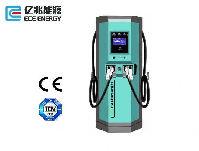
Solar Energy Storage Charger Integrated Solution
[a]https%3A%2F%2Fwww.ecelibattery.com%2Fproducts%2Fsolar-energy-storage-charger-integrated-solution%2F[/a] <br>#off #grid #solar #power #system #battery #bank <br>PV BESS solar based charging station system Combining the photovoltaic garage system, battery energy storage system (BESS) and electric vehicle charging equipment, the monitoring system is integrated in one. Make full use of public space, environmental protection power generation. The photovoltaic power generation system first provides power for loads such as charging piles, and stores the excess electric energy in the commercial solar power storage batteries to supplement when the solar energy system is insufficient. Through the coordination of solar energy and energy storage systems, we can minimize the amount of electricity generated from the grid and reduce electricity bills. <br> <br>Detail of Solar Energy Storage Charger Integrated Solution <br>Solar carport <br>The solar carport is a dual purpose structure that can shelter vehicles while using the sun to produce clean, renewable energy. This free electricity can be used on site and (or) used to charge the EV fleet. Solar carport can increase land value and create revenue opportunities for field operators through electric vehicle charging points, brands and advertising. <br> <br>Charging Pile <br>OCPP integration. <br>Dynamic intelligent DC power sharing technology <br>Remote diagnostics, repair and updates <br>Easily connect to Charging points Management System <br> <br>Support Ethernet, QR scanning to enter APP for charging transaction. Support extended GPRS communication. <br>Multiple charging modes are optional according to time, quantity, amount, Autofill and so on. <br>A 7-inch display screen can display the charging status in real time. <br>There are three charging state indication including power supply, charging, fault. <br> <br>Integrated Outdoor BESS <br>215 KWh outdoor integrated energy storage cabinet, combined with photovoltaic power generation system to realize self-use and saving. <br>The system is equipped with battery, PCS, EMS, and a one-stop solution for easy installation and maintenance. <br>Support multi-machine parallel, can be freely expanded, to meet a variety of use scenarios. <br> <br>System Operation Logic of Industrial Solar Battery Storage <br> <br>DC bus solution of PV BESS solar charging station for electronics <br>The DC bus solution of PV BESS car solar charging station adopts the architecture of DC bus power supply for DC bus. It transforms the DC power from grid,PV system, Battery into the matching voltage range with the charging of new energy vehicles through the DC / DC charging module. <br> <br>DC coupling to reduce the loss of direct intersection transformation <br> <br>Photovoltaic direct supply charging pile to improve the utilization rate of new energy <br> <br>Energy storage system, peak load shifting and valley filling, reduce the distribution capacity of the power grid <br> <br>Solve the problem of power distribution and capacity expansion <br> <br>DC Bus Solution of Pv Bess mobile solar charging station <br> <br>AC Bus Solution of PV BESS solar powered electric charging stations <br>The AC bus solution of PV BESS EV charging station is a commonly used optical storage and charging solution, which is widely used in the application of charging station system expansion and complementary application of the system. <br> <br>PV system, energy storage, battery integrated container solution <br> <br>Large access power range, flexible design <br> <br>It can be used for micro-grid applications such as power supply, electricity sales in industrial parks, large charging stations and other applications <br> <br>The energy storage system can participate in peak load shifting and valley filling, reduce the distribution capacity of the power grid, and solve the problem of distribution capacity expansion <br> <br>For more information about off grid solar power system battery bank and solar car charging station cost, please feel free to contact us!

LQW18AN2N2D00D
[a]https%3A%2F%2Fwww.zkhk-ic.com%2Fproducts%2Flqw18an2n2d00d.html[/a] <br>#lqw18an2n2d00d <br>LQW18AN2N2D00D Overview <br>The SMD inductor LQW18AN2N2D00D is a chip inductor that is designed to be used in a variety of electronic applications. <br> <br>This inductor has a compact design and features a small footprint, making it ideal for use in devices where space is at a premium. It is also highly reliable and has a long service life, thanks to its high-quality construction materials and design. <br> <br>The LQW18AN2N2D00D inductor has a nominal inductance of 2.2nH and a rated current of 1.5A. It operates at a frequency range of up to 2.4GHz and has a DC resistance of 0.04Ω. The inductor has a tolerance of ±0.3nH and is RoHS compliant. <br> <br>Overall, the SMD inductor LQW18AN2N2D00D is an excellent choice for use in a wide range of electronic devices and systems, including mobile devices, telecommunications equipment, audio and video equipment, and more. Its compact size, high reliability, and excellent performance make it a highly desirable component for many different applications. <br> <br>ZKHK distributes active and passive electronic component china of various internationally renowned brands, especially in non-volatile memory Flash, F-RAM, EEPROM and wireless memory/RFID, etc. [A1]. Its applications involve wireless communication, telecommunication equipment, enterprise network, digital media, home entertainment, automotive electronics, industrial control and many other fields; at the same time, it also provides customers with unpopular and military-grade component products.
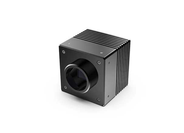
GH-SW640Pro-U3 SWIR Camera
#small #ir #camera <br>GH-SW640Pro-U3 SWIR Camera <br>The SWIR Camera series feature a 640 x 512 pixel InGaAs focal plane array (FPA) with a pitch of 15μm. The camera operates in the 900nm – 1700nm wavelength range, which covers the SWIR region of the spectrum. The product has the characteristics of small size, high reliability and excellent environmental adaptability. The product adopts USB3.0 interface, and users can integrate it into the application system quickly and easily. <br> <br>The camera is a high-performance usb3.0 SWIR camera that offers high sensitivity, low noise, and high resolution for imaging in low-light-level conditions. With its advanced features and capabilities, this usb 3.0 camera is an ideal choice for various applications such as surveillance, astronomy, machine vision, industrial process monitoring, and medical imaging. <br> <br>High Frame Rate <br> <br>TE Cooler <br> <br>Low Readout Noise & Power Consumption <br> <br>Windowing <br> <br>TECHNICAL SPECIFICATION OF GH-SW640PRO-U3 SWIR CAMERA <br>Key Specs <br>Model type GH-SW640Pro-U3 <br>Dark Current HG: 26.5e MG: 42.8e LG: 400e <br>Full Well Capacity HG: 8.5Ke MG: 63.9Ke LG: 1.5Me <br>Data Interface USB3.0 <br>Sensor GH-SW640Pro <br>Shutter Mode Global Shutter <br>Active Area 9.6mm x 7.2mm <br>Resolution 640 x 512 <br>Pixel Size 15μm <br>Frame Rate 430Hz <br>Integration Time 40μs ~ 1s <br>Pixel format Mono <br>Spectral Response 900nm ~ 1700nm <br>Dynamic Range 69.8dB <br>SNR 62.42dB <br>Pixel Bit Depth 8/14 bit <br>Power Input 12V DC, 4.8W(TEC Off) <br>Cooling Method TEC <br>Dimension(L x W x H) 55mm x 55mm x 60mm <br>Lens Mount C-Mount <br>Operating Temp. -40 ℃ ~ +60 ℃ <br>Weight <250g <br>Certificate CE, FCC, RoHS <br> <br>Now as a leading SWIR technology company in Asian, the 14,000 square feet fabrication department operates in an ISO 9001:2008 certified fabrication facility that contains several III-V foundries with Class 100 to 100,000 cleanrooms for wafer fabrication, chip packaging, and device testing. GHOPTO’s engineering team can take your optoelectronics fabrication needs from process design, through development stages, and eventually to commercial production in-house. With our world-class design and fabrication facility, GHOPTO is ready to take your next project from design to prototype to volume production. <br> <br>[a]https%3A%2F%2Fwww.ghopto.com%2Fproducts%2Fgh-sw640pro-u3-gh-sw640pro-cl-swir-camera%2F[/a]
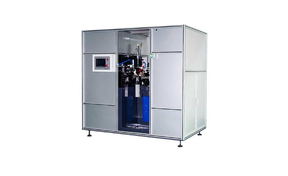
LASER SEAM WELDING
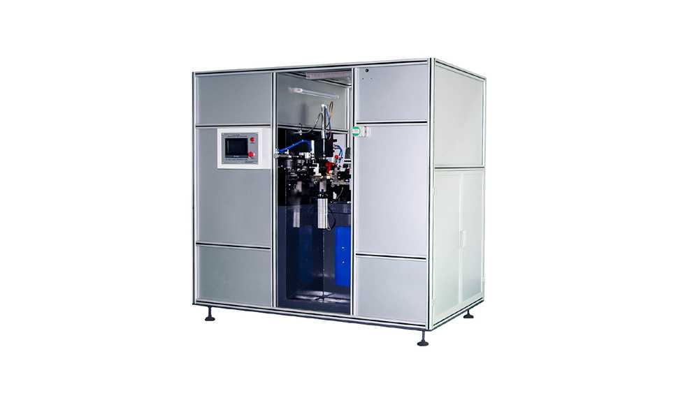
LASER SEAM WELDING <br>Laser seam welding is a superior welding technique that provides precise and efficient joining of two metal sheets without the need for a filler or any post-processing. The laser beam melts the overlapping sheets together, creating a clean and smooth weld seam. Laser seam welder technology ensures a high degree of accuracy, allowing for the creation of contact-free and uniform weld seams. Unlike traditional welding methods such as MIG and TIG welding, laser seam welding offers the benefit of welding multiple layers of material at once, making it ideal for high-volume production settings. The resulting welded surface is stronger than the initial materials, providing superior durability and resistance to cracking. With the ability to work with a variety of metals, laser seam welding is essential for industries such as automotive, aerospace, and electronics, where welded joints must be precise and of high quality. If you want to know more about laser seam welding, please do not hesitate to contact the Xihe seam welder manufacturer. <br> <br>LASER SEAM WELDING PROVIDED BY XIHE <br>Pot Cover Stainless Steel Belt Laser Welder <br> <br>HOW DOES LASER SEAM WELDING WORK? <br>As an automated seam welding, laser seam welding is a precise welding technique used to join two metal sheets together. The process utilizes a laser beam which melts the edges of the sheets, creating a clean and homogenous weld seam. The welding process can be controlled easily through a computer-based system, ensuring that the weld is conducted with high accuracy and precision. The laser energy is focused through optics, which creates a narrow and intense beam that melts the metal at the welding point. The process is clean and allows for the welding of thin sheets without the need for a filler or post-processing. Ultimately, laser seam welding provides a cost-effective and reliable method for welding that is widely used in industries that require high-quality and precise welded joints. <br> <br>BENEFITS OF LASER SEAM WELDING <br>1 <br>Precision: Laser seam welding offers exceptional accuracy and precision as the focused laser beam ensures that the metal is melted at precisely the right location. This results in a clean and uniform weld with minimal distortion or warping. <br> <br>2 <br>Speed: Laser seam welding is a fast process where the laser beam can move quickly over the metal sheets. This translates to a high production rate, enabling the manufacture of large volumes of welded products in a short period. <br> <br>3 <br>Consistency: Laser seam welding provides excellent consistency in the weld quality. The automated system ensures that the welding parameters remain consistent throughout the process, reducing the risk of defects and achieving a uniform result. <br> <br>4 <br>Efficiency: Laser seam welding is an energy-efficient process that requires less power compared to traditional welding methods. It also eliminates the need for a filler material, resulting in less waste and reducing production costs. <br> <br>AUTOMATED LASER SEAM WELDING SYSTEMS AND PROCESS CONTROL METHODOLOGIES <br>Automated laser seam welding systems use robotic arms and sensors to control and execute the welding process. These systems are used in industries where high production rates, uniformity, and precision are essential. The automated systems can control the laser beam intensity, speed, and other parameters, ensuring that the welding process is conducted accurately and with a high degree of repeatability. <br> <br>Process control methodologies ensure that the automated welding system operates within the desired range of parameters. Monitoring and controlling the welding process require feedback systems that measure the temperature, laser power output, and beam position. Feedback systems can alert the operator if the welding process deviates from the allowable range. Automated systems can also adjust parameters during the welding process to achieve optimal results. <br> <br>Process control also involves quality assurance initiatives, such as inspection and testing of welded parts. Non-destructive testing techniques, such as radiography, ultrasound, and magnetic particle testing, can detect any defects or deviations in the welded parts. <br> <br>Automated laser seam welding systems also offer remote access and monitoring capabilities, which allow operators to monitor the welding process in real-time. The data collected from these advanced systems can be analyzed to identify trends, patterns, and potential areas for improvement, leading to the development of more efficient processes. <br> <br>In summary, automated laser seam welding systems combined with process control methodologies offer an efficient way to execute and monitor welding processes in various industrial applications. With their high precision, accuracy, and uniformity, they reduce defects and increase productivity, ultimately leading to higher quality products and customer satisfaction. <br> <br>COMPARISON OF LASER SEAM WELDING WITH OTHER WELDING TECHNIQUES <br>Laser seam welding is a welding technique that has several advantages compared to other traditional welding techniques, such as TIG (tungsten inert gas) welding, MIG (metal inert gas) welding, and spot welding. <br> <br>One of the primary advantages of laser seam welding is its high precision and accuracy. The laser beam creates tight, narrow weld lines, which results in less distortion and minimal heat-affected zones. This makes it ideal for welding seams in thin sheets of material or in areas that are difficult to access. <br> <br>Laser seam welding is also a fast, efficient process, with speeds that are up to ten times faster than traditional welding methods. This makes it highly suitable for large-scale production in industries such as automotive, aerospace, or medical devices. <br> <br>Furthermore, laser seam welding requires little or no post-weld processing, which reduces the overall production time and costs. In comparison, traditional welding methods require post-weld grinding, cleaning, or polishing, which increases the production lead time and cost. <br> <br>Lastly, laser seam welding is environmentally friendly, as it produces minimal waste and fumes during the welding process. By comparison, traditional welding methods, such as gas welding or electrode arc welding, use consumables such as electrodes and shielding gas that produce waste and emissions. <br> <br>In summary, laser seam welding is an innovative technology that provides high accuracy, fast production rates, reduced post-weld processing, and is environmentally friendly. These features make it a preferred choice for different applications over conventional welding methods. <br> <br>Hot laser seam welding provided by xihe:1000 watt laser welder. <br> <br>APPLICATIONS OF LASER SEAM WELDING <br>FIRST <br>Automotive Industry: Laser seam welding is widely used in the automotive industry for welding car body components, such as doors, hoods, and fenders. It provides precise and consistent welds that are strong and long-lasting, improving both the safety and durability of the vehicles. <br> <br>SECOND <br>Medical Device Industry: Laser seam welding is utilized in the medical device industry for welding metal parts of implants and surgical tools. This technique offers precise and uniform welds that ensure the quality and safety of the medical equipment. <br> <br>Aerospace Industry: Laser seam welding is increasingly used in the aerospace industry for welding precision components and structures. This technique enables the fabrication of complex shapes and high... <br> <br>THIRD <br>Aerospace Industry: Laser seam welding is increasingly used in the aerospace industry for welding precision components and structures. This technique enables the fabrication of complex shapes and high-quality welds, making it ideal in the production of aircraft parts that require high strength and precision. <br> <br>Now the price of seam welder for sale is reasonable, if you have needs, please contact us. <br> <br>As one of laser welding machine manufacturers, we will do our best to meet all the needs of customers.
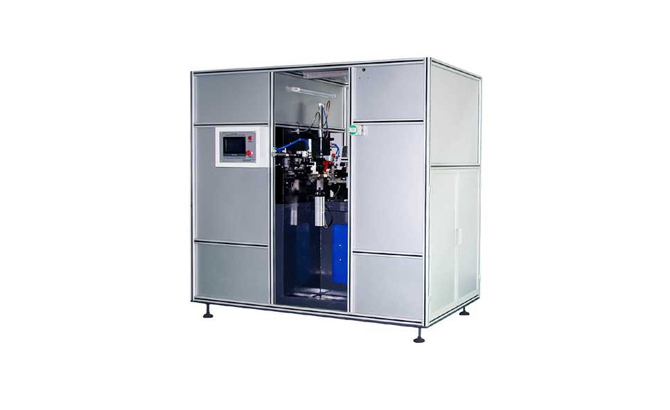
LASER SEAM WELDING
LASER SEAM WELDING <br>Laser seam welding is a superior welding technique that provides precise and efficient joining of two metal sheets without the need for a filler or any post-processing. The laser beam melts the overlapping sheets together, creating a clean and smooth weld seam. Laser seam welder technology ensures a high degree of accuracy, allowing for the creation of contact-free and uniform weld seams. Unlike traditional welding methods such as MIG and TIG welding, laser seam welding offers the benefit of welding multiple layers of material at once, making it ideal for high-volume production settings. The resulting welded surface is stronger than the initial materials, providing superior durability and resistance to cracking. With the ability to work with a variety of metals, laser seam welding is essential for industries such as automotive, aerospace, and electronics, where welded joints must be precise and of high quality. If you want to know more about laser seam welding, please do not hesitate to contact the Xihe seam welder manufacturer. <br> <br>LASER SEAM WELDING PROVIDED BY XIHE <br>Pot Cover Stainless Steel Belt Laser Welder <br> <br>HOW DOES LASER SEAM WELDING WORK? <br>As an automated seam welding, laser seam welding is a precise welding technique used to join two metal sheets together. The process utilizes a laser beam which melts the edges of the sheets, creating a clean and homogenous weld seam. The welding process can be controlled easily through a computer-based system, ensuring that the weld is conducted with high accuracy and precision. The laser energy is focused through optics, which creates a narrow and intense beam that melts the metal at the welding point. The process is clean and allows for the welding of thin sheets without the need for a filler or post-processing. Ultimately, laser seam welding provides a cost-effective and reliable method for welding that is widely used in industries that require high-quality and precise welded joints. <br> <br>BENEFITS OF LASER SEAM WELDING <br>1 <br>Precision: Laser seam welding offers exceptional accuracy and precision as the focused laser beam ensures that the metal is melted at precisely the right location. This results in a clean and uniform weld with minimal distortion or warping. <br> <br>2 <br>Speed: Laser seam welding is a fast process where the laser beam can move quickly over the metal sheets. This translates to a high production rate, enabling the manufacture of large volumes of welded products in a short period. <br> <br>3 <br>Consistency: Laser seam welding provides excellent consistency in the weld quality. The automated system ensures that the welding parameters remain consistent throughout the process, reducing the risk of defects and achieving a uniform result. <br> <br>4 <br>Efficiency: Laser seam welding is an energy-efficient process that requires less power compared to traditional welding methods. It also eliminates the need for a filler material, resulting in less waste and reducing production costs. <br> <br>AUTOMATED LASER SEAM WELDING SYSTEMS AND PROCESS CONTROL METHODOLOGIES <br>Automated laser seam welding systems use robotic arms and sensors to control and execute the welding process. These systems are used in industries where high production rates, uniformity, and precision are essential. The automated systems can control the laser beam intensity, speed, and other parameters, ensuring that the welding process is conducted accurately and with a high degree of repeatability. <br> <br>Process control methodologies ensure that the automated welding system operates within the desired range of parameters. Monitoring and controlling the welding process require feedback systems that measure the temperature, laser power output, and beam position. Feedback systems can alert the operator if the welding process deviates from the allowable range. Automated systems can also adjust parameters during the welding process to achieve optimal results. <br> <br>Process control also involves quality assurance initiatives, such as inspection and testing of welded parts. Non-destructive testing techniques, such as radiography, ultrasound, and magnetic particle testing, can detect any defects or deviations in the welded parts. <br> <br>Automated laser seam welding systems also offer remote access and monitoring capabilities, which allow operators to monitor the welding process in real-time. The data collected from these advanced systems can be analyzed to identify trends, patterns, and potential areas for improvement, leading to the development of more efficient processes. <br> <br>In summary, automated laser seam welding systems combined with process control methodologies offer an efficient way to execute and monitor welding processes in various industrial applications. With their high precision, accuracy, and uniformity, they reduce defects and increase productivity, ultimately leading to higher quality products and customer satisfaction. <br> <br>COMPARISON OF LASER SEAM WELDING WITH OTHER WELDING TECHNIQUES <br>Laser seam welding is a welding technique that has several advantages compared to other traditional welding techniques, such as TIG (tungsten inert gas) welding, MIG (metal inert gas) welding, and spot welding. <br> <br>One of the primary advantages of laser seam welding is its high precision and accuracy. The laser beam creates tight, narrow weld lines, which results in less distortion and minimal heat-affected zones. This makes it ideal for welding seams in thin sheets of material or in areas that are difficult to access. <br> <br>Laser seam welding is also a fast, efficient process, with speeds that are up to ten times faster than traditional welding methods. This makes it highly suitable for large-scale production in industries such as automotive, aerospace, or medical devices. <br> <br>Furthermore, laser seam welding requires little or no post-weld processing, which reduces the overall production time and costs. In comparison, traditional welding methods require post-weld grinding, cleaning, or polishing, which increases the production lead time and cost. <br> <br>Lastly, laser seam welding is environmentally friendly, as it produces minimal waste and fumes during the welding process. By comparison, traditional welding methods, such as gas welding or electrode arc welding, use consumables such as electrodes and shielding gas that produce waste and emissions. <br> <br>In summary, laser seam welding is an innovative technology that provides high accuracy, fast production rates, reduced post-weld processing, and is environmentally friendly. These features make it a preferred choice for different applications over conventional welding methods. <br> <br>Hot laser seam welding provided by xihe:1000 watt laser welder. <br> <br>APPLICATIONS OF LASER SEAM WELDING <br>FIRST <br>Automotive Industry: Laser seam welding is widely used in the automotive industry for welding car body components, such as doors, hoods, and fenders. It provides precise and consistent welds that are strong and long-lasting, improving both the safety and durability of the vehicles. <br> <br>SECOND <br>Medical Device Industry: Laser seam welding is utilized in the medical device industry for welding metal parts of implants and surgical tools. This technique offers precise and uniform welds that ensure the quality and safety of the medical equipment. <br> <br>Aerospace Industry: Laser seam welding is increasingly used in the aerospace industry for welding precision components and structures. This technique enables the fabrication of complex shapes and high... <br> <br>THIRD <br>Aerospace Industry: Laser seam welding is increasingly used in the aerospace industry for welding precision components and structures. This technique enables the fabrication of complex shapes and high-quality welds, making it ideal in the production of aircraft parts that require high strength and precision. <br> <br>Now the price of seam welder for sale is reasonable, if you have needs, please contact us. <br> <br>As one of laser welding machine manufacturers, we will do our best to meet all the needs of customers.
LASER SEAM WELDING
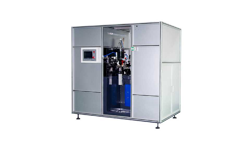
LASER SEAM WELDING <br>Laser seam welding is a superior welding technique that provides precise and efficient joining of two metal sheets without the need for a filler or any post-processing. The laser beam melts the overlapping sheets together, creating a clean and smooth weld seam. Laser seam welder technology ensures a high degree of accuracy, allowing for the creation of contact-free and uniform weld seams. Unlike traditional welding methods such as MIG and TIG welding, laser seam welding offers the benefit of welding multiple layers of material at once, making it ideal for high-volume production settings. The resulting welded surface is stronger than the initial materials, providing superior durability and resistance to cracking. With the ability to work with a variety of metals, laser seam welding is essential for industries such as automotive, aerospace, and electronics, where welded joints must be precise and of high quality. If you want to know more about laser seam welding, please do not hesitate to contact the Xihe seam welder manufacturer. <br> <br>LASER SEAM WELDING PROVIDED BY XIHE <br>Pot Cover Stainless Steel Belt Laser Welder <br> <br>HOW DOES LASER SEAM WELDING WORK? <br>As an automated seam welding, laser seam welding is a precise welding technique used to join two metal sheets together. The process utilizes a laser beam which melts the edges of the sheets, creating a clean and homogenous weld seam. The welding process can be controlled easily through a computer-based system, ensuring that the weld is conducted with high accuracy and precision. The laser energy is focused through optics, which creates a narrow and intense beam that melts the metal at the welding point. The process is clean and allows for the welding of thin sheets without the need for a filler or post-processing. Ultimately, laser seam welding provides a cost-effective and reliable method for welding that is widely used in industries that require high-quality and precise welded joints. <br> <br>BENEFITS OF LASER SEAM WELDING <br>1 <br>Precision: Laser seam welding offers exceptional accuracy and precision as the focused laser beam ensures that the metal is melted at precisely the right location. This results in a clean and uniform weld with minimal distortion or warping. <br> <br>2 <br>Speed: Laser seam welding is a fast process where the laser beam can move quickly over the metal sheets. This translates to a high production rate, enabling the manufacture of large volumes of welded products in a short period. <br> <br>3 <br>Consistency: Laser seam welding provides excellent consistency in the weld quality. The automated system ensures that the welding parameters remain consistent throughout the process, reducing the risk of defects and achieving a uniform result. <br> <br>4 <br>Efficiency: Laser seam welding is an energy-efficient process that requires less power compared to traditional welding methods. It also eliminates the need for a filler material, resulting in less waste and reducing production costs. <br> <br>AUTOMATED LASER SEAM WELDING SYSTEMS AND PROCESS CONTROL METHODOLOGIES <br>Automated laser seam welding systems use robotic arms and sensors to control and execute the welding process. These systems are used in industries where high production rates, uniformity, and precision are essential. The automated systems can control the laser beam intensity, speed, and other parameters, ensuring that the welding process is conducted accurately and with a high degree of repeatability. <br> <br>Process control methodologies ensure that the automated welding system operates within the desired range of parameters. Monitoring and controlling the welding process require feedback systems that measure the temperature, laser power output, and beam position. Feedback systems can alert the operator if the welding process deviates from the allowable range. Automated systems can also adjust parameters during the welding process to achieve optimal results. <br> <br>Process control also involves quality assurance initiatives, such as inspection and testing of welded parts. Non-destructive testing techniques, such as radiography, ultrasound, and magnetic particle testing, can detect any defects or deviations in the welded parts. <br> <br>Automated laser seam welding systems also offer remote access and monitoring capabilities, which allow operators to monitor the welding process in real-time. The data collected from these advanced systems can be analyzed to identify trends, patterns, and potential areas for improvement, leading to the development of more efficient processes. <br> <br>In summary, automated laser seam welding systems combined with process control methodologies offer an efficient way to execute and monitor welding processes in various industrial applications. With their high precision, accuracy, and uniformity, they reduce defects and increase productivity, ultimately leading to higher quality products and customer satisfaction. <br> <br>COMPARISON OF LASER SEAM WELDING WITH OTHER WELDING TECHNIQUES <br>Laser seam welding is a welding technique that has several advantages compared to other traditional welding techniques, such as TIG (tungsten inert gas) welding, MIG (metal inert gas) welding, and spot welding. <br> <br>One of the primary advantages of laser seam welding is its high precision and accuracy. The laser beam creates tight, narrow weld lines, which results in less distortion and minimal heat-affected zones. This makes it ideal for welding seams in thin sheets of material or in areas that are difficult to access. <br> <br>Laser seam welding is also a fast, efficient process, with speeds that are up to ten times faster than traditional welding methods. This makes it highly suitable for large-scale production in industries such as automotive, aerospace, or medical devices. <br> <br>Furthermore, laser seam welding requires little or no post-weld processing, which reduces the overall production time and costs. In comparison, traditional welding methods require post-weld grinding, cleaning, or polishing, which increases the production lead time and cost. <br> <br>Lastly, laser seam welding is environmentally friendly, as it produces minimal waste and fumes during the welding process. By comparison, traditional welding methods, such as gas welding or electrode arc welding, use consumables such as electrodes and shielding gas that produce waste and emissions. <br> <br>In summary, laser seam welding is an innovative technology that provides high accuracy, fast production rates, reduced post-weld processing, and is environmentally friendly. These features make it a preferred choice for different applications over conventional welding methods. <br> <br>Hot laser seam welding provided by xihe:1000 watt laser welder. <br> <br>APPLICATIONS OF LASER SEAM WELDING <br>FIRST <br>Automotive Industry: Laser seam welding is widely used in the automotive industry for welding car body components, such as doors, hoods, and fenders. It provides precise and consistent welds that are strong and long-lasting, improving both the safety and durability of the vehicles. <br> <br>SECOND <br>Medical Device Industry: Laser seam welding is utilized in the medical device industry for welding metal parts of implants and surgical tools. This technique offers precise and uniform welds that ensure the quality and safety of the medical equipment. <br> <br>Aerospace Industry: Laser seam welding is increasingly used in the aerospace industry for welding precision components and structures. This technique enables the fabrication of complex shapes and high... <br> <br>THIRD <br>Aerospace Industry: Laser seam welding is increasingly used in the aerospace industry for welding precision components and structures. This technique enables the fabrication of complex shapes and high-quality welds, making it ideal in the production of aircraft parts that require high strength and precision. <br> <br>Now the price of seam welder for sale is reasonable, if you have needs, please contact us. <br> <br>As one of laser welding machine manufacturers, we will do our best to meet all the needs of customers.
LASER SEAM WELDING
LASER SEAM WELDING <br>Laser seam welding is a superior welding technique that provides precise and efficient joining of two metal sheets without the need for a filler or any post-processing. The laser beam melts the overlapping sheets together, creating a clean and smooth weld seam. Laser seam welder technology ensures a high degree of accuracy, allowing for the creation of contact-free and uniform weld seams. Unlike traditional welding methods such as MIG and TIG welding, laser seam welding offers the benefit of welding multiple layers of material at once, making it ideal for high-volume production settings. The resulting welded surface is stronger than the initial materials, providing superior durability and resistance to cracking. With the ability to work with a variety of metals, laser seam welding is essential for industries such as automotive, aerospace, and electronics, where welded joints must be precise and of high quality. If you want to know more about laser seam welding, please do not hesitate to contact the Xihe seam welder manufacturer. <br> <br>LASER SEAM WELDING PROVIDED BY XIHE <br>Pot Cover Stainless Steel Belt Laser Welder <br> <br>HOW DOES LASER SEAM WELDING WORK? <br>As an automated seam welding, laser seam welding is a precise welding technique used to join two metal sheets together. The process utilizes a laser beam which melts the edges of the sheets, creating a clean and homogenous weld seam. The welding process can be controlled easily through a computer-based system, ensuring that the weld is conducted with high accuracy and precision. The laser energy is focused through optics, which creates a narrow and intense beam that melts the metal at the welding point. The process is clean and allows for the welding of thin sheets without the need for a filler or post-processing. Ultimately, laser seam welding provides a cost-effective and reliable method for welding that is widely used in industries that require high-quality and precise welded joints. <br> <br>BENEFITS OF LASER SEAM WELDING <br>1 <br>Precision: Laser seam welding offers exceptional accuracy and precision as the focused laser beam ensures that the metal is melted at precisely the right location. This results in a clean and uniform weld with minimal distortion or warping. <br> <br>2 <br>Speed: Laser seam welding is a fast process where the laser beam can move quickly over the metal sheets. This translates to a high production rate, enabling the manufacture of large volumes of welded products in a short period. <br> <br>3 <br>Consistency: Laser seam welding provides excellent consistency in the weld quality. The automated system ensures that the welding parameters remain consistent throughout the process, reducing the risk of defects and achieving a uniform result. <br> <br>4 <br>Efficiency: Laser seam welding is an energy-efficient process that requires less power compared to traditional welding methods. It also eliminates the need for a filler material, resulting in less waste and reducing production costs. <br> <br>AUTOMATED LASER SEAM WELDING SYSTEMS AND PROCESS CONTROL METHODOLOGIES <br>Automated laser seam welding systems use robotic arms and sensors to control and execute the welding process. These systems are used in industries where high production rates, uniformity, and precision are essential. The automated systems can control the laser beam intensity, speed, and other parameters, ensuring that the welding process is conducted accurately and with a high degree of repeatability. <br> <br>Process control methodologies ensure that the automated welding system operates within the desired range of parameters. Monitoring and controlling the welding process require feedback systems that measure the temperature, laser power output, and beam position. Feedback systems can alert the operator if the welding process deviates from the allowable range. Automated systems can also adjust parameters during the welding process to achieve optimal results. <br> <br>Process control also involves quality assurance initiatives, such as inspection and testing of welded parts. Non-destructive testing techniques, such as radiography, ultrasound, and magnetic particle testing, can detect any defects or deviations in the welded parts. <br> <br>Automated laser seam welding systems also offer remote access and monitoring capabilities, which allow operators to monitor the welding process in real-time. The data collected from these advanced systems can be analyzed to identify trends, patterns, and potential areas for improvement, leading to the development of more efficient processes. <br> <br>In summary, automated laser seam welding systems combined with process control methodologies offer an efficient way to execute and monitor welding processes in various industrial applications. With their high precision, accuracy, and uniformity, they reduce defects and increase productivity, ultimately leading to higher quality products and customer satisfaction. <br> <br>COMPARISON OF LASER SEAM WELDING WITH OTHER WELDING TECHNIQUES <br>Laser seam welding is a welding technique that has several advantages compared to other traditional welding techniques, such as TIG (tungsten inert gas) welding, MIG (metal inert gas) welding, and spot welding. <br> <br>One of the primary advantages of laser seam welding is its high precision and accuracy. The laser beam creates tight, narrow weld lines, which results in less distortion and minimal heat-affected zones. This makes it ideal for welding seams in thin sheets of material or in areas that are difficult to access. <br> <br>Laser seam welding is also a fast, efficient process, with speeds that are up to ten times faster than traditional welding methods. This makes it highly suitable for large-scale production in industries such as automotive, aerospace, or medical devices. <br> <br>Furthermore, laser seam welding requires little or no post-weld processing, which reduces the overall production time and costs. In comparison, traditional welding methods require post-weld grinding, cleaning, or polishing, which increases the production lead time and cost. <br> <br>Lastly, laser seam welding is environmentally friendly, as it produces minimal waste and fumes during the welding process. By comparison, traditional welding methods, such as gas welding or electrode arc welding, use consumables such as electrodes and shielding gas that produce waste and emissions. <br> <br>In summary, laser seam welding is an innovative technology that provides high accuracy, fast production rates, reduced post-weld processing, and is environmentally friendly. These features make it a preferred choice for different applications over conventional welding methods. <br> <br>Hot laser seam welding provided by xihe:1000 watt laser welder. <br> <br>APPLICATIONS OF LASER SEAM WELDING <br>FIRST <br>Automotive Industry: Laser seam welding is widely used in the automotive industry for welding car body components, such as doors, hoods, and fenders. It provides precise and consistent welds that are strong and long-lasting, improving both the safety and durability of the vehicles. <br> <br>SECOND <br>Medical Device Industry: Laser seam welding is utilized in the medical device industry for welding metal parts of implants and surgical tools. This technique offers precise and uniform welds that ensure the quality and safety of the medical equipment. <br> <br>Aerospace Industry: Laser seam welding is increasingly used in the aerospace industry for welding precision components and structures. This technique enables the fabrication of complex shapes and high... <br> <br>THIRD <br>Aerospace Industry: Laser seam welding is increasingly used in the aerospace industry for welding precision components and structures. This technique enables the fabrication of complex shapes and high-quality welds, making it ideal in the production of aircraft parts that require high strength and precision. <br> <br>Now the price of seam welder for sale is reasonable, if you have needs, please contact us. <br> <br>As one of laser welding machine manufacturers, we will do our best to meet all the needs of customers.
PCB Assembly Service
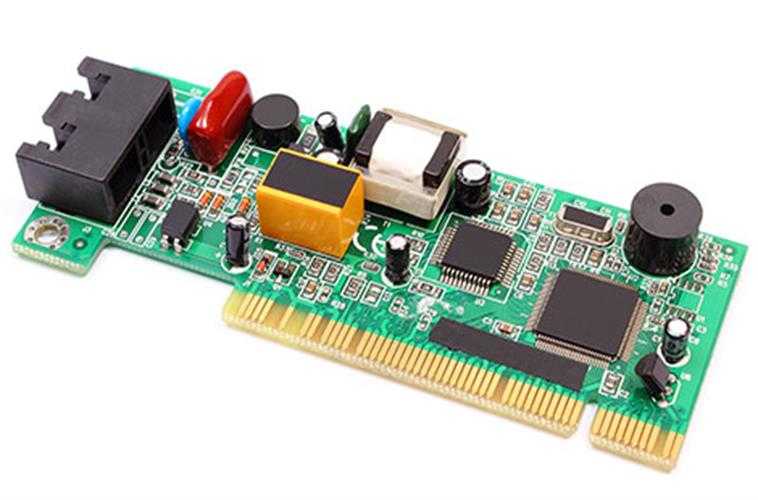
[a]https%3A%2F%2Fwww.greenpcba.com%2Fpcb-assembly-service%2F[/a] <br>#printed #circuit #assembly <br> <br>GreensTone specializes in the pcba pcb assembly, including: <br>Circuit board assembly <br>Surface mount technologies (SMT) <br>Pin Through Hole <br>Complex secondary operations <br>Automated conformal coating <br>Inspection <br>Automated optical inspection (AOI) <br> <br>GreensTone conducts upfront evaluations of all components, designs and fabrication processes to optimize suppliers and technologies. We recommend appropriate alternatives to minimize risks and reduce costs. <br> <br>GreensTone is a cost-effective electronic contract manufacturing company providing one-stop contract electronic assembly services. Our services include: PCB manufacturing, Electronic component sourcing, printed circuit board pcba assembly, chip programming, confirmal coating, cable assembly, CNC/injection molding service, plastic/metal case assembly, and final testing. <br> <br>GreensTone focused on: <br>PCB assembly <br>Box build assembly <br>One-stop contract electronics manufacturing&assembly <br> <br>GreensTone specialized in: <br>SMT, Through-hole <br>Full PCB components procurement, <br>Contract PCB assembly OEM <br>CNC, plastic injection molding, sheet metal fabrication <br>Box build assembly <br> <br>How Long Does It Take To Assemble A PCB? <br>Depending on the production quantities, PCB production takes 3-14 business days. For prototype run, it takes 3-5 business days. For volume run, it normall takes 14 business days. pcba circuit board assembly normally take 5-14 business days for small to medium volume production. The components lead time is uncertain, and for normal parts, it can be around 2-4weeks, but for long lead time part like some ICs from TI and Microchip, it would be longer. And it will depend on the lead time which the suppliers provide. <br> <br> <br>What does one stop pcb assembly do? A blank PCB soldered with electronic semiconductors and components. GreensTone PCB assembly process is like this: You send us your design file→ we arrange pcb&pcba manufacture and parts sourcing as per your files request →parts receipt→Parts kit preparation →SMD manchine pragraming→paste stencil fabrication→SMD manchine set-up→SMD verification of component's footprints→assemble PCB top side→assemble PCB bottom side→ Through-hole wave solder/hand solder assembly→ Touch up and testing→ Final QC&shipment <br> <br>How Long Does It Take To Assemble A PCB? <br>About GreensTone <br>GreensTone is an contract electronics manufacturing factory providing one-stop electronic assembly services.Our services include PCB manufacturing, parts procurement, PCB assembly, China prototype pcb pcba assembly services, Mechanical fabrication,Plastic molding and box build.We are concentrated on one-stop contract electronics manufacturing in low-medium volume, and products life-cycle management. <br> <br>Since 2011,our company has successfully served customers in the United States, Australia, Western Europe and other regions of the world spanning many areas,like industrial equipments, communication electronics,Traffic control, medical electronics, security, new energy and laser equipments, etc... <br> <br>There are many contract electronics manufacturing companies, but we are one of the best choices for you. <br> <br>For more about printed circuit assembly, contact us.
Miller Audio LLC
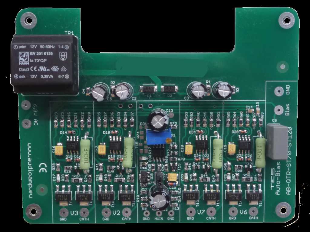
Miller Audio LLC <br>Dallas-Fort Worth Metropolitan Area, TX, USA <br>4255 Peppermill Lane Dallas, TX 75287 <br>972-693-5116 <br>[email protected] <br>Miller Audio LLC, based in Dallas, TX, is a privately held, audio electronics design business. We manufacture specialized vacuum tube audio equipment for vintage and new production products. We develop and manufacture audio upgrades for vintage vacuum tube amplifiers, integrate automatic bias circuit designs to enhance and extend the service life of vacuum tubes. We manufacture upgrade audio kits, and design and build complete audio amplifiers, ready for use in home or commercial applications.
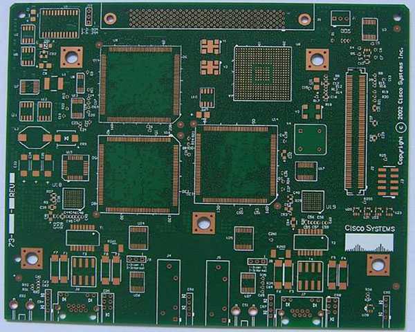
High Density Interconnect PCB from Hitech Circuits
HDI pcb is the abbreviation for High Density Interconnect pcb or High Density pcb. An HDI PCB is defined as a printed circuit board with a higher wiring density per unit area than a conventional PCB. Hitech Circuits Co., Limited is a professional high density interconnect pcbs, hdi pcb board manufacturer, supplier and design company from China, if you are looking for reliable high density interconnect PCb board partner from China, please don’t hesitate to contact [email protected] . <br>What is a high-density interconnection PCB board <br>HDI is the abbreviation of High Density Interconnection, which is a kind of technology for the production of printed circuit boards. High density interconnection PCB board is a circuit board with a relatively high line distribution density using micro-blind and buried via technology. <br> <br>HDI includes the use of fine features or signal traces and spaces of 0.003” (75 µm) or less and laser-drilled blind or buried microvia technology. Microvias allow the use of micro-interconnects from one layer to another within a PCB utilizing a smaller pad diameter creating additional routing density or reducing form factor. <br> <br>HDI pcb board is a compact product designed for small-capacity users. <br> <br>Advantages of high-density interconnected PCB boards <br>It can reduce the cost of PCB: When the density of PCB increases to more than eight-layer board, it is manufactured by HDI, and its cost will be lower than that of the traditional complex pressing process. <br>Increase circuit density: has better interconnection than that of traditional circuit boards and parts <br>Conducive to the use of advanced construction technology <br>Have better electrical performance and signal accuracy <br>Better reliability <br>Can improve thermal properties <br>It can improve radio frequency interference ( RFI ), electromagnetic wave interference ( EMI ), electrostatic discharge ( ESD ) <br>Increase design efficiency <br>Disadvantages of high-density interconnected PCB boards <br>The value of NDI impedance focuses on pattern transfer (complexity of patterns) and pattern electroplating process. <br>The quantity and quality are abnormal, especially the high-density circuit part of the HDI PCB board has a slower etch rate than the isolation line, which causes the isolation line to be over-etched. <br>When the entire HDI board is etched after electroplating, a large area of copper on the PCB circuit board will be etched away, which increases the production cost. At the same time, a large amount of copper ions enter the waste liquid after etching, causing environmental pollution and difficulty in recycling. <br>High-density interconnection PCB board Vs ordinary PCB board <br>Ordinary PCB board is mainly FR-4, which is laminated with epoxy resin and electronic grade glass cloth. Generally, traditional HDI PCB board uses backed copper foil on the outer surface, because laser drilling cannot penetrate the glass cloth, glass fiber-free backed copper foil is generally used. However, the current high-energy laser drilling machine can penetrate 1180 glass cloth. This is no difference from ordinary PCB board materials. <br> <br>Applications of high-density interconnected PCB boards <br>While electronic design is constantly improving the performance of the whole equipment, researchers are also working hard to reduce its size. In small portable products ranging from mobile phones to smart weapons, “small” is an eternal pursuit. High-density interconnection (HDI PCB) technology can make terminal product designs more compact, while meeting higher standards of electronic performance and efficiency. HDI PCB board is widely used in mobile phones, digital cameras, MP3, MP4, notebook computers, automotive electronics, IC carrier boards and other digital products, among which mobile phones are the most widely used. <br> <br>High density PCB is used extensively in applications and industries including <br> <br>Cell phone <br>GPS <br>Telecom <br>Semiconductor <br>Automotive <br>Military <br>Medical <br>Instrumentation <br>Note book computers <br>IC Carrier board <br>Healthcare <br>FAQs for Hitech Circuits on HDI PCBs <br>1. What types of HDI PCBs are available at Hitech Circuits? <br>Hitech Circuits offers a range of HDI PCBs, including those with through vias from surface to surface, with buried vias and through vias, sequential lamination with various materials, and with passive substrate constructions having no electrical connection. Each type caters to specific design and performance requirements. <br> <br>2. Can Hitech Circuits accommodate custom HDI PCB designs? <br>Absolutely! Hitech Circuits specializes in custom HDI PCB designs tailored to meet unique project requirements. Our team works closely with clients to understand their needs and deliver high-quality, precise PCBs that fit their specifications. <br> <br>3. What materials are used in the manufacturing of HDI PCBs? <br>HDI PCBs at Hi-Tech Circuits are made from various high-quality materials, including FR-4, high-frequency materials (such as Rogers and Taconic), and flex and rigid-flex materials. Material selection depends on the application’s requirements, such as thermal management, electrical performance, and mechanical durability. <br> <br>4. How does Hitech Circuits ensure the quality of their HDI PCBs? <br>Quality assurance is paramount at Hitech Circuits. We employ stringent quality control processes at every manufacturing stage, from design and material selection to fabrication and testing. Our HDI PCBs undergo multiple quality checks, including electrical testing, visual inspection, and automated optical inspection (AOI) to ensure they meet the highest standards. <br> <br>5. What are the lead times for HDI PCB production? <br>Lead times for HDI PCB production can vary based on the complexity of the design and the quantity required. Generally, prototype orders can be completed within a few days to two weeks, while larger production orders may take several weeks. We strive to meet our clients’ deadlines and can provide more specific timeframes upon order placement. <br> <br>6. Are there any design guidelines for HDI PCBs I should follow? <br>Yes, Hitech Circuits provides detailed design guidelines for HDI PCBs, which include recommendations on trace width, spacing, via sizes, and layer stacking. These guidelines help ensure the manufacturability of your design and optimize performance. Our team is also available to assist with any design questions. <br> <br>7. Can Hitech Circuits support high-volume HDI PCB orders? <br>Certainly! Hitech Circuits is equipped to handle high-volume orders with the same attention to detail and quality assurance as smaller orders. We have the capacity and expertise to meet the demands of large-scale production runs efficiently. <br> <br>8. How can I get a quote for my HDI PCB project? <br>Getting a quote is easy! Visit our website, and fill out the quote request form with your project details, such as PCB specifications, quantity, and any special requirements. Our sales team will review your information and provide you with a detailed quote promptly.
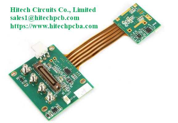
Rigid-flex PCB manufacturer up to 18 layers Rigid Flex Board Manufacturer & Assembly – One-stop service
What are Rigid-Flex Circuit Boards? <br> <br>As the name implies, a Rigid-Flex PCB is a hybrid of a Flex PCB and a Rigid PCB. The combination of the two types of boards utilises the benefits each one provides, integrating the versatility of the flexible board with the robustness of the rigid board. Rigid-flex printed circuit boards are used in more complex mechanical designs, eliminating flexible cables and wiring and replacing it with integrated circuits. <br> <br>Rigid-Flex PCBs, by definition, are a combination of rigid part(s) joined by interconnecting flex areas where the flex material is used across the entire PCB area. <br> <br>The rigid parts are where there is no bending requirement. Again, PTHs take connections from layer to layer as required. Rigid-flex may also employ other technologies as required eg. HDI. Unlike the cost-effective flex PCBs, Rigid-Flex PCBs can be a bit more costly due to their intricate design. <br> <br>Rigid-flex PCB design can be used to eliminate or greatly reduce requirements for bulky and costly cable harnesses, in turn taking out costs and reducing assembly time. Like the pure flexible PCBs, a high volume of rigid-flex PCBs are used in aviation and space applications – and also in automotive and test equipment. <br> <br>Rigid-Flex Pcb <br> <br>The flexible layers of a Rigid-Flex PCB are buried within the board and penetrate through the rigid sections of the PCB. <br> <br>The trend to miniaturization in electronics continues. Integrated circuit board solutions are becoming more and more popular as a means of efficiently utilizing the even smaller casing volume in all three dimensions. <br> <br>A rigid-flex printed circuit board is unique as the rigid part of the circuitry can be placed directly into the application. Then, the flexible section can be bent and even folded to fit around components to make another direct connection. This aspect ensures a reliable connection to parts for higher performance. <br> <br>Some of the most common products that incorporate rigid-flex PCBs in their design include laptop computers, smartphones, and wearable devices due to the bending capabilities of rigid-flex. <br> <br>Rigid-flex pcb boards are PCBs that have Flexible PCBs (FPC) and Rigid PCBs on the same board, which are commonly employed to save space, remove wiring assemblies and can also be welded with complex components. Combining other higher technology boards, such as HDI, as a part of its packaging, is also a common design. <br> <br>WhatsApp:+8618118703950 <br>For RFQ,please contact [email protected]
Rigid-flex PCB manufacturer up to 18 layers
What are Rigid-Flex Circuit Boards? <br> <br>As the name implies, a Rigid-Flex PCB is a hybrid of a Flex PCB and a Rigid PCB. The combination of the two types of boards utilises the benefits each one provides, integrating the versatility of the flexible board with the robustness of the rigid board. Rigid-flex printed circuit boards are used in more complex mechanical designs, eliminating flexible cables and wiring and replacing it with integrated circuits. <br> <br>Rigid-Flex PCBs, by definition, are a combination of rigid part(s) joined by interconnecting flex areas where the flex material is used across the entire PCB area. <br> <br>The rigid parts are where there is no bending requirement. Again, PTHs take connections from layer to layer as required. Rigid-flex may also employ other technologies as required eg. HDI. Unlike the cost-effective flex PCBs, Rigid-Flex PCBs can be a bit more costly due to their intricate design. <br> <br>Rigid-flex PCB design can be used to eliminate or greatly reduce requirements for bulky and costly cable harnesses, in turn taking out costs and reducing assembly time. Like the pure flexible PCBs, a high volume of rigid-flex PCBs are used in aviation and space applications – and also in automotive and test equipment. <br> <br>The flexible layers of a Rigid-Flex PCB are buried within the board and penetrate through the rigid sections of the PCB. <br> <br>The trend to miniaturization in electronics continues. Integrated circuit board solutions are becoming more and more popular as a means of efficiently utilizing the even smaller casing volume in all three dimensions. <br> <br>A rigid-flex printed circuit board is unique as the rigid part of the circuitry can be placed directly into the application. Then, the flexible section can be bent and even folded to fit around components to make another direct connection. This aspect ensures a reliable connection to parts for higher performance. <br> <br>Some of the most common products that incorporate rigid-flex PCBs in their design include laptop computers, smartphones, and wearable devices due to the bending capabilities of rigid-flex. <br> <br>Rigid-flex pcb boards are PCBs that have Flexible PCBs (FPC) and Rigid PCBs on the same board, which are commonly employed to save space, remove wiring assemblies and can also be welded with complex components. Combining other higher technology boards, such as HDI, as a part of its packaging, is also a common design. <br> <br>Rigid Flex PCB design <br> <br>The designs of Rigid Flex PCBs are a little more complex as these boards are designed in 3D, which allows the board to be folded or twisted to create the desired shape for the product. Designing a board in 3D means they can offer greater spatial efficiency and can subsequently be used in special instances where space and weight reduction may be necessary, such as in medical devices. By being able to design in three dimensions designers can twist, fold and roll the flexible board substrates to achieve their desired shape for the final application's package. <br> <br>Rigid Flex PCBs are usually thinner than other boards, meaning it’s a great option for any thin or light packaging needs your products may have. With thin copper layers and adhesive-less laminates, it’s a great small, thin and light solution for your circuit design needs. <br> <br>Rigid-Flex PCBs Fabrication Applications: <br> <br>Rigid-Flex PCBs offer a wide array of applications, ranging from smart devices to cell phones and digital cameras. Increasingly, rigid-flex board fabrication has been used in medical devices such as pacemakers for their space and weight reduction capabilities. The same advantages for rigid-flex PCB usage can be applied to smart control systems. <br> <br>In consumer products, rigid-flex doesn't just maximize space and weight but greatly improves reliability, eliminating many needs for solder joints and delicate, fragile wiring that are prone to connection issues. These are just some examples, but Rigid-Flex PCBs can be used to benefit nearly all advanced electrical applications including testing equipment, tools and automobiles. <br> <br>Rigid-Flex PCB and Its Production Process <br> <br>The development of FPC and PCB has spawned a new product that is called rigid-flex PCB. Therefore, rigid- flex PCB is according to the relevant process requirements and through the lamination process to combine rigid board and flex board to form a circuit board with FPC characteristics and PCB characteristics. <br> <br>Because rigid-flex PCB has a variety of complex structural forms, the manufacturing process is also different. Below picture shows the regular rigid-flex PCB and an example for regular stack up design. <br> <br>Rigid flex PCB production is based on below steps: the first step is to process the rigid outer cover layer. The electroplating graphic that needs to be pressed in the outer layer, and then through the CNC milling machine, punching or laser method, routing out or routing the half of depth of the flexible part which is located in rigid layer. Flex board and the rigid outer cover are boned by adhesive sheet. The adhesive sheet has been pre-opened in the flexible part. <br> <br>During the lamination process, if the rigid outer layer uses routing structure, a suitable pressure filling board should be prepared for the flex part. Using a vacuum pressing machine to obtain better press quality, and meanwhile with some auxiliary coating materials, such as PE, etc., so that the pressing process can provide a uniform pressure on the entire board, and make the low -flowing sticky sheet is fully flowing and filling the gap, especially for complex structures. Before adhesion or lamination, appropriate baking should be done as needed to remove moisture. <br> <br>After lamination, the rigid- flex PCB can use a through hole treatment process which is similar to a multi-layer rigid board, the different part is remove drilling dirt. The method of removing drilling dirt depends on what materials used. Like the rigid board, drilling the hole after fully baking, and then use the plasma etching process to remove the residue in the hole wall. Before the plasma is treated, bake is also needed to remove water vapor. Caval polyesterness is generally recommended to not exceed 13um. The pore -plating process of conventional rigid board can be used, but the specific process parameters of the electroplating should be determined according to the reliability test data of the pores. <br> <br>The next process is similar to the multi -layer rigid board. The outer layer etching, covering membrane (welded film), surface treatment, etc. can be used in similar processes. When making outline of the rigid-flex PCB, remove the filling board in the flexible part or depth control rigid outer cover in the flexible area can be formed into a rigid-flex PCB. <br> <br>Careful consideration of Rigid-Flex solutions and a proper assessment of the available options at the early stages in the rigid-flex PCB design phase will return significant benefits. The Rigid-Flex PCBs fabricator must be involved early in the design process to ensure the design and fab portions are both in coordination and to account for final product variations. <br> <br>The Rigid-Flex manufacturing phase is also more complex and time-consuming than rigid board fabrication. All the flexible components of the Rigid-Flex assembly have completely different handling, etching, and soldering processes than rigid FR4 boards. <br> <br>Benefits of Rigid Flex PCB <br> <br>Space requirements can be minimized by applying 3D <br> <br>By removing the need for connectors and cables between the individual rigid parts the board size and overall system weight can be reduced. <br> <br>By maximizing space, there is often a lower count in parts. <br> <br>Less solder joints assure higher connection reliability. <br> <br>Handling during assembly is easier in comparison with flexible boards. <br> <br>Simplified PCB assembly processes. <br> <br>Integrated ZIF contacts provide simple modular interfaces to the system environment. <br> <br>Test conditions are simplified. A complete test prior to installation becomes possible. <br> <br>Logistical and assembly costs are significantly reduced with flex-rigid boards. <br> <br>It is possible to increase the complexity of mechanical designs, which also improves the degree of freedom for optimized housing solutions. <br> <br>Rigid Flex PCB Fabrication Applications <br> <br>Rigid flexible PCBs offer a wide array of applications, ranging from military weaponry and aerospace systems to cell phones and digital cameras. Increasingly, rigid flex board fabrication has been used in medical devices such as pacemakers for their space and weight reduction capabilities. The same advantages for rigid flex PCB usage can be applied to military weaponry and weapon control systems <br> <br>In consumer products, rigid flex doesn't just maximize space and weight but greatly improves reliability, eliminating many needs for solder joints and delicate, fragile wiring that are prone to connection issues. These are just some examples, but rigid flex PCBs can be used to benefit nearly all advanced electrical applications including testing equipment, tools and automobiles. <br> <br>Available structures for rigid flex PCB <br> <br>There are numerous, different structures available. The more common ones are defined below: <br> <br>Traditional rigid flex construction (IPC-6013 type 4) Multilayer rigid and flexible circuit combination containing three or more layers with plated through holes. <br> <br>Asymmetrical rigid flex construction, where the FPC is situated on the outer layer of the rigid construction. Containing three or more layers with plated through holes. <br> <br>Multilayer rigid flex construction with buried / blind via (microvia) as part of the rigid construction. 2 layers of microvia are achievable. Construction may also include two rigid structures as part of a homogeneous build. <br> <br>Rigid Flex Printed Circuit Board Manufacturer <br> <br>Rigid flex printed circuit boards (PCBs) are manufactured by combining rigid and flexible board technologies. These circuit boards are made up of multiple flexible circuit inner layers. An epoxy pre-preg bonding film is used to attach together these inner layers. The key benefit of these boards is that they are a combination of the best quality of flexible and rigid circuit boards. This can have several further benefits as far as stability, assembly, signal transmission, and overall size of the circuit are concerned. Hitechpcb provides a number of variants in rigid flex PCBs, which include 4 layer rigid flex with ENIG finish, 10 layer rigid flex with 4 layer flex, 12 layer rigid flex with heat sink, 14 layer rigid flex circuit boards, and many more. It is one of the leading rigid flex PCB manufacturers. <br> <br>Every printed circuit board depends on the copper for carrying electricity. We understand that copper thickness plays a key role in the performance of these circuit boards. Thus, we allow the customers to choose from a variety of copper thicknesses, including 0.5 OZ, 1.0 OZ, 2.0 OZ, 3.0 OZ, up to 6 OZ. The solder mask helps in improving the aesthetic appeal of the components on the PCB. We can provide rigid flex printed circuit boards in various solder mask colors, including white, black, blue, green, red, and Taiyo PSR4000 white. The PCB can be availed in silkscreen colors – black and white. <br> <br>Rigid flex printed circuit boards have minimal space requirements that are optimized by 3D application. These circuit boards require no cables or connectors between the rigid parts. This helps reduce the board size, as well as overall system weight. These lesser solder joints also help assure high connectivity. Additionally, these boards have ZIF contacts that are integrated. These contacts help simplify the system interfacing. This 4 layer rigid flex PCB and other printed circuit boards are vacuum packed during the transit. This helps us assure the quality, as well as working condition of the boards. <br> <br>The Disadvantage and Advantage of Rigid-Flex PCB <br> <br>Rigid-flex PCB has many production processes with the characteristic of superior difficulty in production and high defect rate. Its biggest disadvantage is that the price is more expensive than flex PCB or rigid PCB and long production cycle. Another disadvantage is that both SMT and furnaces may need to use carrier to support the flex PCB which virtually increases the SMT cost. <br> <br>One of the key features of rigid-flex PCB is the thin profile and changeable shape, making it an ideal solution for ultra -thin and ultra -light packaging. Although the rigid flex PCB may be more expensive in design and manufacturing, they do have many advantages and can solve many problems in traditional hardboard technology. <br> <br>1. Small Size and Flexible Shape <br> <br>The rigid- flex PCB is easier to install more components in smaller space, because they can change the shape according to a specific contour. This technology will reduce the size and weight of the final product and the overall system cost. At the same time, the compact shape of rigid flex PCB makes it the best choice for fine lines and high -density circuits in HDI technology. <br> <br>2. Customized for Different Applications <br> <br>Rigid-flex PCB has various packages, which can be customized for the application of many industries such as aerospace, military, medical equipment and consumer electronics. They can customize the size and shape to adapt to the shell design and 3D design, which provides designers with more possibilities to meet different requirements in specific applications. <br> <br>3. Better Mechanical Stability <br> <br>The stability of the rigid board and the flexibility of the flexible board form the stable structure of the entire packaging, while retaining the reliability and flexibility required for small space installation. <br> <br>4. Good Performance in Harsh Environments <br> <br>Rigid-flex PCB has high resistance and high vibration capacity, so they can work normally in a high -stress environment. There are fewer cables and connectors used in rigid-flexible PCB, which also reduces security risks and maintenance in future use. <br> <br>5. Easy to Manufacture and Test <br> <br>The rigid-flex PCB requires a small number of inter connect and related components/parts. It helps simplify the assembly operation, making rigid –flex PCB easier to assemble and test. Rigid-flex PCB is very suitable for PCB prototypes. <br> <br>In addition to the above advantages, other common advantages of rigid-flex PCB also include high circuit density, good heat dissipation and good chemical resistance. In a word, rigid-flex PCB combines all the advantages of rigid PCB and flex PCB, and at the same time make up for the shortcomings. This PCB is the best solution to design reliable and powerful circuits for smart wearable devices and other industries. <br> <br>[a]https%3A%2F%2Fwww.hitechpcba.com%2Frigid-flex-pcb-manufacturer[/a]
Solar Energy Storage Charger Integrated Solution
[a]https%3A%2F%2Fwww.ecelibattery.com%2Fproducts%2Fsolar-energy-storage-charger-integrated-solution%2F[/a] <br>#off #grid #solar #power #system #battery #bank <br>PV BESS solar based charging station system Combining the photovoltaic garage system, battery energy storage system (BESS) and electric vehicle charging equipment, the monitoring system is integrated in one. Make full use of public space, environmental protection power generation. The photovoltaic power generation system first provides power for loads such as charging piles, and stores the excess electric energy in the commercial solar power storage batteries to supplement when the solar energy system is insufficient. Through the coordination of solar energy and energy storage systems, we can minimize the amount of electricity generated from the grid and reduce electricity bills. <br> <br>Detail of Solar Energy Storage Charger Integrated Solution <br>Solar carport <br>The solar carport is a dual purpose structure that can shelter vehicles while using the sun to produce clean, renewable energy. This free electricity can be used on site and (or) used to charge the EV fleet. Solar carport can increase land value and create revenue opportunities for field operators through electric vehicle charging points, brands and advertising. <br> <br>Charging Pile <br>OCPP integration. <br>Dynamic intelligent DC power sharing technology <br>Remote diagnostics, repair and updates <br>Easily connect to Charging points Management System <br> <br>Support Ethernet, QR scanning to enter APP for charging transaction. Support extended GPRS communication. <br>Multiple charging modes are optional according to time, quantity, amount, Autofill and so on. <br>A 7-inch display screen can display the charging status in real time. <br>There are three charging state indication including power supply, charging, fault. <br> <br>Integrated Outdoor BESS <br>215 KWh outdoor integrated energy storage cabinet, combined with photovoltaic power generation system to realize self-use and saving. <br>The system is equipped with battery, PCS, EMS, and a one-stop solution for easy installation and maintenance. <br>Support multi-machine parallel, can be freely expanded, to meet a variety of use scenarios. <br> <br>System Operation Logic of Industrial Solar Battery Storage <br> <br>DC bus solution of PV BESS solar charging station for electronics <br>The DC bus solution of PV BESS car solar charging station adopts the architecture of DC bus power supply for DC bus. It transforms the DC power from grid,PV system, Battery into the matching voltage range with the charging of new energy vehicles through the DC / DC charging module. <br> <br>DC coupling to reduce the loss of direct intersection transformation <br> <br>Photovoltaic direct supply charging pile to improve the utilization rate of new energy <br> <br>Energy storage system, peak load shifting and valley filling, reduce the distribution capacity of the power grid <br> <br>Solve the problem of power distribution and capacity expansion <br> <br>DC Bus Solution of Pv Bess mobile solar charging station <br> <br>AC Bus Solution of PV BESS solar powered electric charging stations <br>The AC bus solution of PV BESS EV charging station is a commonly used optical storage and charging solution, which is widely used in the application of charging station system expansion and complementary application of the system. <br> <br>PV system, energy storage, battery integrated container solution <br> <br>Large access power range, flexible design <br> <br>It can be used for micro-grid applications such as power supply, electricity sales in industrial parks, large charging stations and other applications <br> <br>The energy storage system can participate in peak load shifting and valley filling, reduce the distribution capacity of the power grid, and solve the problem of distribution capacity expansion <br> <br>For more information about off grid solar power system battery bank and solar car charging station cost, please feel free to contact us!
LQW18AN2N2D00D
[a]https%3A%2F%2Fwww.zkhk-ic.com%2Fproducts%2Flqw18an2n2d00d.html[/a] <br>#lqw18an2n2d00d <br>LQW18AN2N2D00D Overview <br>The SMD inductor LQW18AN2N2D00D is a chip inductor that is designed to be used in a variety of electronic applications. <br> <br>This inductor has a compact design and features a small footprint, making it ideal for use in devices where space is at a premium. It is also highly reliable and has a long service life, thanks to its high-quality construction materials and design. <br> <br>The LQW18AN2N2D00D inductor has a nominal inductance of 2.2nH and a rated current of 1.5A. It operates at a frequency range of up to 2.4GHz and has a DC resistance of 0.04Ω. The inductor has a tolerance of ±0.3nH and is RoHS compliant. <br> <br>Overall, the SMD inductor LQW18AN2N2D00D is an excellent choice for use in a wide range of electronic devices and systems, including mobile devices, telecommunications equipment, audio and video equipment, and more. Its compact size, high reliability, and excellent performance make it a highly desirable component for many different applications. <br> <br>ZKHK distributes active and passive electronic component china of various internationally renowned brands, especially in non-volatile memory Flash, F-RAM, EEPROM and wireless memory/RFID, etc. [A1]. Its applications involve wireless communication, telecommunication equipment, enterprise network, digital media, home entertainment, automotive electronics, industrial control and many other fields; at the same time, it also provides customers with unpopular and military-grade component products.
GH-SW640Pro-U3 SWIR Camera
#small #ir #camera <br>GH-SW640Pro-U3 SWIR Camera <br>The SWIR Camera series feature a 640 x 512 pixel InGaAs focal plane array (FPA) with a pitch of 15μm. The camera operates in the 900nm – 1700nm wavelength range, which covers the SWIR region of the spectrum. The product has the characteristics of small size, high reliability and excellent environmental adaptability. The product adopts USB3.0 interface, and users can integrate it into the application system quickly and easily. <br> <br>The camera is a high-performance usb3.0 SWIR camera that offers high sensitivity, low noise, and high resolution for imaging in low-light-level conditions. With its advanced features and capabilities, this usb 3.0 camera is an ideal choice for various applications such as surveillance, astronomy, machine vision, industrial process monitoring, and medical imaging. <br> <br>High Frame Rate <br> <br>TE Cooler <br> <br>Low Readout Noise & Power Consumption <br> <br>Windowing <br> <br>TECHNICAL SPECIFICATION OF GH-SW640PRO-U3 SWIR CAMERA <br>Key Specs <br>Model type GH-SW640Pro-U3 <br>Dark Current HG: 26.5e MG: 42.8e LG: 400e <br>Full Well Capacity HG: 8.5Ke MG: 63.9Ke LG: 1.5Me <br>Data Interface USB3.0 <br>Sensor GH-SW640Pro <br>Shutter Mode Global Shutter <br>Active Area 9.6mm x 7.2mm <br>Resolution 640 x 512 <br>Pixel Size 15μm <br>Frame Rate 430Hz <br>Integration Time 40μs ~ 1s <br>Pixel format Mono <br>Spectral Response 900nm ~ 1700nm <br>Dynamic Range 69.8dB <br>SNR 62.42dB <br>Pixel Bit Depth 8/14 bit <br>Power Input 12V DC, 4.8W(TEC Off) <br>Cooling Method TEC <br>Dimension(L x W x H) 55mm x 55mm x 60mm <br>Lens Mount C-Mount <br>Operating Temp. -40 ℃ ~ +60 ℃ <br>Weight <250g <br>Certificate CE, FCC, RoHS <br> <br>Now as a leading SWIR technology company in Asian, the 14,000 square feet fabrication department operates in an ISO 9001:2008 certified fabrication facility that contains several III-V foundries with Class 100 to 100,000 cleanrooms for wafer fabrication, chip packaging, and device testing. GHOPTO’s engineering team can take your optoelectronics fabrication needs from process design, through development stages, and eventually to commercial production in-house. With our world-class design and fabrication facility, GHOPTO is ready to take your next project from design to prototype to volume production. <br> <br>[a]https%3A%2F%2Fwww.ghopto.com%2Fproducts%2Fgh-sw640pro-u3-gh-sw640pro-cl-swir-camera%2F[/a]
LASER SEAM WELDING
LASER SEAM WELDING <br>Laser seam welding is a superior welding technique that provides precise and efficient joining of two metal sheets without the need for a filler or any post-processing. The laser beam melts the overlapping sheets together, creating a clean and smooth weld seam. Laser seam welder technology ensures a high degree of accuracy, allowing for the creation of contact-free and uniform weld seams. Unlike traditional welding methods such as MIG and TIG welding, laser seam welding offers the benefit of welding multiple layers of material at once, making it ideal for high-volume production settings. The resulting welded surface is stronger than the initial materials, providing superior durability and resistance to cracking. With the ability to work with a variety of metals, laser seam welding is essential for industries such as automotive, aerospace, and electronics, where welded joints must be precise and of high quality. If you want to know more about laser seam welding, please do not hesitate to contact the Xihe seam welder manufacturer. <br> <br>LASER SEAM WELDING PROVIDED BY XIHE <br>Pot Cover Stainless Steel Belt Laser Welder <br> <br>HOW DOES LASER SEAM WELDING WORK? <br>As an automated seam welding, laser seam welding is a precise welding technique used to join two metal sheets together. The process utilizes a laser beam which melts the edges of the sheets, creating a clean and homogenous weld seam. The welding process can be controlled easily through a computer-based system, ensuring that the weld is conducted with high accuracy and precision. The laser energy is focused through optics, which creates a narrow and intense beam that melts the metal at the welding point. The process is clean and allows for the welding of thin sheets without the need for a filler or post-processing. Ultimately, laser seam welding provides a cost-effective and reliable method for welding that is widely used in industries that require high-quality and precise welded joints. <br> <br>BENEFITS OF LASER SEAM WELDING <br>1 <br>Precision: Laser seam welding offers exceptional accuracy and precision as the focused laser beam ensures that the metal is melted at precisely the right location. This results in a clean and uniform weld with minimal distortion or warping. <br> <br>2 <br>Speed: Laser seam welding is a fast process where the laser beam can move quickly over the metal sheets. This translates to a high production rate, enabling the manufacture of large volumes of welded products in a short period. <br> <br>3 <br>Consistency: Laser seam welding provides excellent consistency in the weld quality. The automated system ensures that the welding parameters remain consistent throughout the process, reducing the risk of defects and achieving a uniform result. <br> <br>4 <br>Efficiency: Laser seam welding is an energy-efficient process that requires less power compared to traditional welding methods. It also eliminates the need for a filler material, resulting in less waste and reducing production costs. <br> <br>AUTOMATED LASER SEAM WELDING SYSTEMS AND PROCESS CONTROL METHODOLOGIES <br>Automated laser seam welding systems use robotic arms and sensors to control and execute the welding process. These systems are used in industries where high production rates, uniformity, and precision are essential. The automated systems can control the laser beam intensity, speed, and other parameters, ensuring that the welding process is conducted accurately and with a high degree of repeatability. <br> <br>Process control methodologies ensure that the automated welding system operates within the desired range of parameters. Monitoring and controlling the welding process require feedback systems that measure the temperature, laser power output, and beam position. Feedback systems can alert the operator if the welding process deviates from the allowable range. Automated systems can also adjust parameters during the welding process to achieve optimal results. <br> <br>Process control also involves quality assurance initiatives, such as inspection and testing of welded parts. Non-destructive testing techniques, such as radiography, ultrasound, and magnetic particle testing, can detect any defects or deviations in the welded parts. <br> <br>Automated laser seam welding systems also offer remote access and monitoring capabilities, which allow operators to monitor the welding process in real-time. The data collected from these advanced systems can be analyzed to identify trends, patterns, and potential areas for improvement, leading to the development of more efficient processes. <br> <br>In summary, automated laser seam welding systems combined with process control methodologies offer an efficient way to execute and monitor welding processes in various industrial applications. With their high precision, accuracy, and uniformity, they reduce defects and increase productivity, ultimately leading to higher quality products and customer satisfaction. <br> <br>COMPARISON OF LASER SEAM WELDING WITH OTHER WELDING TECHNIQUES <br>Laser seam welding is a welding technique that has several advantages compared to other traditional welding techniques, such as TIG (tungsten inert gas) welding, MIG (metal inert gas) welding, and spot welding. <br> <br>One of the primary advantages of laser seam welding is its high precision and accuracy. The laser beam creates tight, narrow weld lines, which results in less distortion and minimal heat-affected zones. This makes it ideal for welding seams in thin sheets of material or in areas that are difficult to access. <br> <br>Laser seam welding is also a fast, efficient process, with speeds that are up to ten times faster than traditional welding methods. This makes it highly suitable for large-scale production in industries such as automotive, aerospace, or medical devices. <br> <br>Furthermore, laser seam welding requires little or no post-weld processing, which reduces the overall production time and costs. In comparison, traditional welding methods require post-weld grinding, cleaning, or polishing, which increases the production lead time and cost. <br> <br>Lastly, laser seam welding is environmentally friendly, as it produces minimal waste and fumes during the welding process. By comparison, traditional welding methods, such as gas welding or electrode arc welding, use consumables such as electrodes and shielding gas that produce waste and emissions. <br> <br>In summary, laser seam welding is an innovative technology that provides high accuracy, fast production rates, reduced post-weld processing, and is environmentally friendly. These features make it a preferred choice for different applications over conventional welding methods. <br> <br>Hot laser seam welding provided by xihe:1000 watt laser welder. <br> <br>APPLICATIONS OF LASER SEAM WELDING <br>FIRST <br>Automotive Industry: Laser seam welding is widely used in the automotive industry for welding car body components, such as doors, hoods, and fenders. It provides precise and consistent welds that are strong and long-lasting, improving both the safety and durability of the vehicles. <br> <br>SECOND <br>Medical Device Industry: Laser seam welding is utilized in the medical device industry for welding metal parts of implants and surgical tools. This technique offers precise and uniform welds that ensure the quality and safety of the medical equipment. <br> <br>Aerospace Industry: Laser seam welding is increasingly used in the aerospace industry for welding precision components and structures. This technique enables the fabrication of complex shapes and high... <br> <br>THIRD <br>Aerospace Industry: Laser seam welding is increasingly used in the aerospace industry for welding precision components and structures. This technique enables the fabrication of complex shapes and high-quality welds, making it ideal in the production of aircraft parts that require high strength and precision. <br> <br>Now the price of seam welder for sale is reasonable, if you have needs, please contact us. <br> <br>As one of laser welding machine manufacturers, we will do our best to meet all the needs of customers.
LASER SEAM WELDING
LASER SEAM WELDING <br>Laser seam welding is a superior welding technique that provides precise and efficient joining of two metal sheets without the need for a filler or any post-processing. The laser beam melts the overlapping sheets together, creating a clean and smooth weld seam. Laser seam welder technology ensures a high degree of accuracy, allowing for the creation of contact-free and uniform weld seams. Unlike traditional welding methods such as MIG and TIG welding, laser seam welding offers the benefit of welding multiple layers of material at once, making it ideal for high-volume production settings. The resulting welded surface is stronger than the initial materials, providing superior durability and resistance to cracking. With the ability to work with a variety of metals, laser seam welding is essential for industries such as automotive, aerospace, and electronics, where welded joints must be precise and of high quality. If you want to know more about laser seam welding, please do not hesitate to contact the Xihe seam welder manufacturer. <br> <br>LASER SEAM WELDING PROVIDED BY XIHE <br>Pot Cover Stainless Steel Belt Laser Welder <br> <br>HOW DOES LASER SEAM WELDING WORK? <br>As an automated seam welding, laser seam welding is a precise welding technique used to join two metal sheets together. The process utilizes a laser beam which melts the edges of the sheets, creating a clean and homogenous weld seam. The welding process can be controlled easily through a computer-based system, ensuring that the weld is conducted with high accuracy and precision. The laser energy is focused through optics, which creates a narrow and intense beam that melts the metal at the welding point. The process is clean and allows for the welding of thin sheets without the need for a filler or post-processing. Ultimately, laser seam welding provides a cost-effective and reliable method for welding that is widely used in industries that require high-quality and precise welded joints. <br> <br>BENEFITS OF LASER SEAM WELDING <br>1 <br>Precision: Laser seam welding offers exceptional accuracy and precision as the focused laser beam ensures that the metal is melted at precisely the right location. This results in a clean and uniform weld with minimal distortion or warping. <br> <br>2 <br>Speed: Laser seam welding is a fast process where the laser beam can move quickly over the metal sheets. This translates to a high production rate, enabling the manufacture of large volumes of welded products in a short period. <br> <br>3 <br>Consistency: Laser seam welding provides excellent consistency in the weld quality. The automated system ensures that the welding parameters remain consistent throughout the process, reducing the risk of defects and achieving a uniform result. <br> <br>4 <br>Efficiency: Laser seam welding is an energy-efficient process that requires less power compared to traditional welding methods. It also eliminates the need for a filler material, resulting in less waste and reducing production costs. <br> <br>AUTOMATED LASER SEAM WELDING SYSTEMS AND PROCESS CONTROL METHODOLOGIES <br>Automated laser seam welding systems use robotic arms and sensors to control and execute the welding process. These systems are used in industries where high production rates, uniformity, and precision are essential. The automated systems can control the laser beam intensity, speed, and other parameters, ensuring that the welding process is conducted accurately and with a high degree of repeatability. <br> <br>Process control methodologies ensure that the automated welding system operates within the desired range of parameters. Monitoring and controlling the welding process require feedback systems that measure the temperature, laser power output, and beam position. Feedback systems can alert the operator if the welding process deviates from the allowable range. Automated systems can also adjust parameters during the welding process to achieve optimal results. <br> <br>Process control also involves quality assurance initiatives, such as inspection and testing of welded parts. Non-destructive testing techniques, such as radiography, ultrasound, and magnetic particle testing, can detect any defects or deviations in the welded parts. <br> <br>Automated laser seam welding systems also offer remote access and monitoring capabilities, which allow operators to monitor the welding process in real-time. The data collected from these advanced systems can be analyzed to identify trends, patterns, and potential areas for improvement, leading to the development of more efficient processes. <br> <br>In summary, automated laser seam welding systems combined with process control methodologies offer an efficient way to execute and monitor welding processes in various industrial applications. With their high precision, accuracy, and uniformity, they reduce defects and increase productivity, ultimately leading to higher quality products and customer satisfaction. <br> <br>COMPARISON OF LASER SEAM WELDING WITH OTHER WELDING TECHNIQUES <br>Laser seam welding is a welding technique that has several advantages compared to other traditional welding techniques, such as TIG (tungsten inert gas) welding, MIG (metal inert gas) welding, and spot welding. <br> <br>One of the primary advantages of laser seam welding is its high precision and accuracy. The laser beam creates tight, narrow weld lines, which results in less distortion and minimal heat-affected zones. This makes it ideal for welding seams in thin sheets of material or in areas that are difficult to access. <br> <br>Laser seam welding is also a fast, efficient process, with speeds that are up to ten times faster than traditional welding methods. This makes it highly suitable for large-scale production in industries such as automotive, aerospace, or medical devices. <br> <br>Furthermore, laser seam welding requires little or no post-weld processing, which reduces the overall production time and costs. In comparison, traditional welding methods require post-weld grinding, cleaning, or polishing, which increases the production lead time and cost. <br> <br>Lastly, laser seam welding is environmentally friendly, as it produces minimal waste and fumes during the welding process. By comparison, traditional welding methods, such as gas welding or electrode arc welding, use consumables such as electrodes and shielding gas that produce waste and emissions. <br> <br>In summary, laser seam welding is an innovative technology that provides high accuracy, fast production rates, reduced post-weld processing, and is environmentally friendly. These features make it a preferred choice for different applications over conventional welding methods. <br> <br>Hot laser seam welding provided by xihe:1000 watt laser welder. <br> <br>APPLICATIONS OF LASER SEAM WELDING <br>FIRST <br>Automotive Industry: Laser seam welding is widely used in the automotive industry for welding car body components, such as doors, hoods, and fenders. It provides precise and consistent welds that are strong and long-lasting, improving both the safety and durability of the vehicles. <br> <br>SECOND <br>Medical Device Industry: Laser seam welding is utilized in the medical device industry for welding metal parts of implants and surgical tools. This technique offers precise and uniform welds that ensure the quality and safety of the medical equipment. <br> <br>Aerospace Industry: Laser seam welding is increasingly used in the aerospace industry for welding precision components and structures. This technique enables the fabrication of complex shapes and high... <br> <br>THIRD <br>Aerospace Industry: Laser seam welding is increasingly used in the aerospace industry for welding precision components and structures. This technique enables the fabrication of complex shapes and high-quality welds, making it ideal in the production of aircraft parts that require high strength and precision. <br> <br>Now the price of seam welder for sale is reasonable, if you have needs, please contact us. <br> <br>As one of laser welding machine manufacturers, we will do our best to meet all the needs of customers.
LASER SEAM WELDING
LASER SEAM WELDING <br>Laser seam welding is a superior welding technique that provides precise and efficient joining of two metal sheets without the need for a filler or any post-processing. The laser beam melts the overlapping sheets together, creating a clean and smooth weld seam. Laser seam welder technology ensures a high degree of accuracy, allowing for the creation of contact-free and uniform weld seams. Unlike traditional welding methods such as MIG and TIG welding, laser seam welding offers the benefit of welding multiple layers of material at once, making it ideal for high-volume production settings. The resulting welded surface is stronger than the initial materials, providing superior durability and resistance to cracking. With the ability to work with a variety of metals, laser seam welding is essential for industries such as automotive, aerospace, and electronics, where welded joints must be precise and of high quality. If you want to know more about laser seam welding, please do not hesitate to contact the Xihe seam welder manufacturer. <br> <br>LASER SEAM WELDING PROVIDED BY XIHE <br>Pot Cover Stainless Steel Belt Laser Welder <br> <br>HOW DOES LASER SEAM WELDING WORK? <br>As an automated seam welding, laser seam welding is a precise welding technique used to join two metal sheets together. The process utilizes a laser beam which melts the edges of the sheets, creating a clean and homogenous weld seam. The welding process can be controlled easily through a computer-based system, ensuring that the weld is conducted with high accuracy and precision. The laser energy is focused through optics, which creates a narrow and intense beam that melts the metal at the welding point. The process is clean and allows for the welding of thin sheets without the need for a filler or post-processing. Ultimately, laser seam welding provides a cost-effective and reliable method for welding that is widely used in industries that require high-quality and precise welded joints. <br> <br>BENEFITS OF LASER SEAM WELDING <br>1 <br>Precision: Laser seam welding offers exceptional accuracy and precision as the focused laser beam ensures that the metal is melted at precisely the right location. This results in a clean and uniform weld with minimal distortion or warping. <br> <br>2 <br>Speed: Laser seam welding is a fast process where the laser beam can move quickly over the metal sheets. This translates to a high production rate, enabling the manufacture of large volumes of welded products in a short period. <br> <br>3 <br>Consistency: Laser seam welding provides excellent consistency in the weld quality. The automated system ensures that the welding parameters remain consistent throughout the process, reducing the risk of defects and achieving a uniform result. <br> <br>4 <br>Efficiency: Laser seam welding is an energy-efficient process that requires less power compared to traditional welding methods. It also eliminates the need for a filler material, resulting in less waste and reducing production costs. <br> <br>AUTOMATED LASER SEAM WELDING SYSTEMS AND PROCESS CONTROL METHODOLOGIES <br>Automated laser seam welding systems use robotic arms and sensors to control and execute the welding process. These systems are used in industries where high production rates, uniformity, and precision are essential. The automated systems can control the laser beam intensity, speed, and other parameters, ensuring that the welding process is conducted accurately and with a high degree of repeatability. <br> <br>Process control methodologies ensure that the automated welding system operates within the desired range of parameters. Monitoring and controlling the welding process require feedback systems that measure the temperature, laser power output, and beam position. Feedback systems can alert the operator if the welding process deviates from the allowable range. Automated systems can also adjust parameters during the welding process to achieve optimal results. <br> <br>Process control also involves quality assurance initiatives, such as inspection and testing of welded parts. Non-destructive testing techniques, such as radiography, ultrasound, and magnetic particle testing, can detect any defects or deviations in the welded parts. <br> <br>Automated laser seam welding systems also offer remote access and monitoring capabilities, which allow operators to monitor the welding process in real-time. The data collected from these advanced systems can be analyzed to identify trends, patterns, and potential areas for improvement, leading to the development of more efficient processes. <br> <br>In summary, automated laser seam welding systems combined with process control methodologies offer an efficient way to execute and monitor welding processes in various industrial applications. With their high precision, accuracy, and uniformity, they reduce defects and increase productivity, ultimately leading to higher quality products and customer satisfaction. <br> <br>COMPARISON OF LASER SEAM WELDING WITH OTHER WELDING TECHNIQUES <br>Laser seam welding is a welding technique that has several advantages compared to other traditional welding techniques, such as TIG (tungsten inert gas) welding, MIG (metal inert gas) welding, and spot welding. <br> <br>One of the primary advantages of laser seam welding is its high precision and accuracy. The laser beam creates tight, narrow weld lines, which results in less distortion and minimal heat-affected zones. This makes it ideal for welding seams in thin sheets of material or in areas that are difficult to access. <br> <br>Laser seam welding is also a fast, efficient process, with speeds that are up to ten times faster than traditional welding methods. This makes it highly suitable for large-scale production in industries such as automotive, aerospace, or medical devices. <br> <br>Furthermore, laser seam welding requires little or no post-weld processing, which reduces the overall production time and costs. In comparison, traditional welding methods require post-weld grinding, cleaning, or polishing, which increases the production lead time and cost. <br> <br>Lastly, laser seam welding is environmentally friendly, as it produces minimal waste and fumes during the welding process. By comparison, traditional welding methods, such as gas welding or electrode arc welding, use consumables such as electrodes and shielding gas that produce waste and emissions. <br> <br>In summary, laser seam welding is an innovative technology that provides high accuracy, fast production rates, reduced post-weld processing, and is environmentally friendly. These features make it a preferred choice for different applications over conventional welding methods. <br> <br>Hot laser seam welding provided by xihe:1000 watt laser welder. <br> <br>APPLICATIONS OF LASER SEAM WELDING <br>FIRST <br>Automotive Industry: Laser seam welding is widely used in the automotive industry for welding car body components, such as doors, hoods, and fenders. It provides precise and consistent welds that are strong and long-lasting, improving both the safety and durability of the vehicles. <br> <br>SECOND <br>Medical Device Industry: Laser seam welding is utilized in the medical device industry for welding metal parts of implants and surgical tools. This technique offers precise and uniform welds that ensure the quality and safety of the medical equipment. <br> <br>Aerospace Industry: Laser seam welding is increasingly used in the aerospace industry for welding precision components and structures. This technique enables the fabrication of complex shapes and high... <br> <br>THIRD <br>Aerospace Industry: Laser seam welding is increasingly used in the aerospace industry for welding precision components and structures. This technique enables the fabrication of complex shapes and high-quality welds, making it ideal in the production of aircraft parts that require high strength and precision. <br> <br>Now the price of seam welder for sale is reasonable, if you have needs, please contact us. <br> <br>As one of laser welding machine manufacturers, we will do our best to meet all the needs of customers.
LASER SEAM WELDING
LASER SEAM WELDING <br>Laser seam welding is a superior welding technique that provides precise and efficient joining of two metal sheets without the need for a filler or any post-processing. The laser beam melts the overlapping sheets together, creating a clean and smooth weld seam. Laser seam welder technology ensures a high degree of accuracy, allowing for the creation of contact-free and uniform weld seams. Unlike traditional welding methods such as MIG and TIG welding, laser seam welding offers the benefit of welding multiple layers of material at once, making it ideal for high-volume production settings. The resulting welded surface is stronger than the initial materials, providing superior durability and resistance to cracking. With the ability to work with a variety of metals, laser seam welding is essential for industries such as automotive, aerospace, and electronics, where welded joints must be precise and of high quality. If you want to know more about laser seam welding, please do not hesitate to contact the Xihe seam welder manufacturer. <br> <br>LASER SEAM WELDING PROVIDED BY XIHE <br>Pot Cover Stainless Steel Belt Laser Welder <br> <br>HOW DOES LASER SEAM WELDING WORK? <br>As an automated seam welding, laser seam welding is a precise welding technique used to join two metal sheets together. The process utilizes a laser beam which melts the edges of the sheets, creating a clean and homogenous weld seam. The welding process can be controlled easily through a computer-based system, ensuring that the weld is conducted with high accuracy and precision. The laser energy is focused through optics, which creates a narrow and intense beam that melts the metal at the welding point. The process is clean and allows for the welding of thin sheets without the need for a filler or post-processing. Ultimately, laser seam welding provides a cost-effective and reliable method for welding that is widely used in industries that require high-quality and precise welded joints. <br> <br>BENEFITS OF LASER SEAM WELDING <br>1 <br>Precision: Laser seam welding offers exceptional accuracy and precision as the focused laser beam ensures that the metal is melted at precisely the right location. This results in a clean and uniform weld with minimal distortion or warping. <br> <br>2 <br>Speed: Laser seam welding is a fast process where the laser beam can move quickly over the metal sheets. This translates to a high production rate, enabling the manufacture of large volumes of welded products in a short period. <br> <br>3 <br>Consistency: Laser seam welding provides excellent consistency in the weld quality. The automated system ensures that the welding parameters remain consistent throughout the process, reducing the risk of defects and achieving a uniform result. <br> <br>4 <br>Efficiency: Laser seam welding is an energy-efficient process that requires less power compared to traditional welding methods. It also eliminates the need for a filler material, resulting in less waste and reducing production costs. <br> <br>AUTOMATED LASER SEAM WELDING SYSTEMS AND PROCESS CONTROL METHODOLOGIES <br>Automated laser seam welding systems use robotic arms and sensors to control and execute the welding process. These systems are used in industries where high production rates, uniformity, and precision are essential. The automated systems can control the laser beam intensity, speed, and other parameters, ensuring that the welding process is conducted accurately and with a high degree of repeatability. <br> <br>Process control methodologies ensure that the automated welding system operates within the desired range of parameters. Monitoring and controlling the welding process require feedback systems that measure the temperature, laser power output, and beam position. Feedback systems can alert the operator if the welding process deviates from the allowable range. Automated systems can also adjust parameters during the welding process to achieve optimal results. <br> <br>Process control also involves quality assurance initiatives, such as inspection and testing of welded parts. Non-destructive testing techniques, such as radiography, ultrasound, and magnetic particle testing, can detect any defects or deviations in the welded parts. <br> <br>Automated laser seam welding systems also offer remote access and monitoring capabilities, which allow operators to monitor the welding process in real-time. The data collected from these advanced systems can be analyzed to identify trends, patterns, and potential areas for improvement, leading to the development of more efficient processes. <br> <br>In summary, automated laser seam welding systems combined with process control methodologies offer an efficient way to execute and monitor welding processes in various industrial applications. With their high precision, accuracy, and uniformity, they reduce defects and increase productivity, ultimately leading to higher quality products and customer satisfaction. <br> <br>COMPARISON OF LASER SEAM WELDING WITH OTHER WELDING TECHNIQUES <br>Laser seam welding is a welding technique that has several advantages compared to other traditional welding techniques, such as TIG (tungsten inert gas) welding, MIG (metal inert gas) welding, and spot welding. <br> <br>One of the primary advantages of laser seam welding is its high precision and accuracy. The laser beam creates tight, narrow weld lines, which results in less distortion and minimal heat-affected zones. This makes it ideal for welding seams in thin sheets of material or in areas that are difficult to access. <br> <br>Laser seam welding is also a fast, efficient process, with speeds that are up to ten times faster than traditional welding methods. This makes it highly suitable for large-scale production in industries such as automotive, aerospace, or medical devices. <br> <br>Furthermore, laser seam welding requires little or no post-weld processing, which reduces the overall production time and costs. In comparison, traditional welding methods require post-weld grinding, cleaning, or polishing, which increases the production lead time and cost. <br> <br>Lastly, laser seam welding is environmentally friendly, as it produces minimal waste and fumes during the welding process. By comparison, traditional welding methods, such as gas welding or electrode arc welding, use consumables such as electrodes and shielding gas that produce waste and emissions. <br> <br>In summary, laser seam welding is an innovative technology that provides high accuracy, fast production rates, reduced post-weld processing, and is environmentally friendly. These features make it a preferred choice for different applications over conventional welding methods. <br> <br>Hot laser seam welding provided by xihe:1000 watt laser welder. <br> <br>APPLICATIONS OF LASER SEAM WELDING <br>FIRST <br>Automotive Industry: Laser seam welding is widely used in the automotive industry for welding car body components, such as doors, hoods, and fenders. It provides precise and consistent welds that are strong and long-lasting, improving both the safety and durability of the vehicles. <br> <br>SECOND <br>Medical Device Industry: Laser seam welding is utilized in the medical device industry for welding metal parts of implants and surgical tools. This technique offers precise and uniform welds that ensure the quality and safety of the medical equipment. <br> <br>Aerospace Industry: Laser seam welding is increasingly used in the aerospace industry for welding precision components and structures. This technique enables the fabrication of complex shapes and high... <br> <br>THIRD <br>Aerospace Industry: Laser seam welding is increasingly used in the aerospace industry for welding precision components and structures. This technique enables the fabrication of complex shapes and high-quality welds, making it ideal in the production of aircraft parts that require high strength and precision. <br> <br>Now the price of seam welder for sale is reasonable, if you have needs, please contact us. <br> <br>As one of laser welding machine manufacturers, we will do our best to meet all the needs of customers.
PCB Assembly Service
[a]https%3A%2F%2Fwww.greenpcba.com%2Fpcb-assembly-service%2F[/a] <br>#printed #circuit #assembly <br> <br>GreensTone specializes in the pcba pcb assembly, including: <br>Circuit board assembly <br>Surface mount technologies (SMT) <br>Pin Through Hole <br>Complex secondary operations <br>Automated conformal coating <br>Inspection <br>Automated optical inspection (AOI) <br> <br>GreensTone conducts upfront evaluations of all components, designs and fabrication processes to optimize suppliers and technologies. We recommend appropriate alternatives to minimize risks and reduce costs. <br> <br>GreensTone is a cost-effective electronic contract manufacturing company providing one-stop contract electronic assembly services. Our services include: PCB manufacturing, Electronic component sourcing, printed circuit board pcba assembly, chip programming, confirmal coating, cable assembly, CNC/injection molding service, plastic/metal case assembly, and final testing. <br> <br>GreensTone focused on: <br>PCB assembly <br>Box build assembly <br>One-stop contract electronics manufacturing&assembly <br> <br>GreensTone specialized in: <br>SMT, Through-hole <br>Full PCB components procurement, <br>Contract PCB assembly OEM <br>CNC, plastic injection molding, sheet metal fabrication <br>Box build assembly <br> <br>How Long Does It Take To Assemble A PCB? <br>Depending on the production quantities, PCB production takes 3-14 business days. For prototype run, it takes 3-5 business days. For volume run, it normall takes 14 business days. pcba circuit board assembly normally take 5-14 business days for small to medium volume production. The components lead time is uncertain, and for normal parts, it can be around 2-4weeks, but for long lead time part like some ICs from TI and Microchip, it would be longer. And it will depend on the lead time which the suppliers provide. <br> <br> <br>What does one stop pcb assembly do? A blank PCB soldered with electronic semiconductors and components. GreensTone PCB assembly process is like this: You send us your design file→ we arrange pcb&pcba manufacture and parts sourcing as per your files request →parts receipt→Parts kit preparation →SMD manchine pragraming→paste stencil fabrication→SMD manchine set-up→SMD verification of component's footprints→assemble PCB top side→assemble PCB bottom side→ Through-hole wave solder/hand solder assembly→ Touch up and testing→ Final QC&shipment <br> <br>How Long Does It Take To Assemble A PCB? <br>About GreensTone <br>GreensTone is an contract electronics manufacturing factory providing one-stop electronic assembly services.Our services include PCB manufacturing, parts procurement, PCB assembly, China prototype pcb pcba assembly services, Mechanical fabrication,Plastic molding and box build.We are concentrated on one-stop contract electronics manufacturing in low-medium volume, and products life-cycle management. <br> <br>Since 2011,our company has successfully served customers in the United States, Australia, Western Europe and other regions of the world spanning many areas,like industrial equipments, communication electronics,Traffic control, medical electronics, security, new energy and laser equipments, etc... <br> <br>There are many contract electronics manufacturing companies, but we are one of the best choices for you. <br> <br>For more about printed circuit assembly, contact us.
Miller Audio LLC
Miller Audio LLC <br>Dallas-Fort Worth Metropolitan Area, TX, USA <br>4255 Peppermill Lane Dallas, TX 75287 <br>972-693-5116 <br>[email protected] <br>Miller Audio LLC, based in Dallas, TX, is a privately held, audio electronics design business. We manufacture specialized vacuum tube audio equipment for vintage and new production products. We develop and manufacture audio upgrades for vintage vacuum tube amplifiers, integrate automatic bias circuit designs to enhance and extend the service life of vacuum tubes. We manufacture upgrade audio kits, and design and build complete audio amplifiers, ready for use in home or commercial applications.
High Density Interconnect PCB from Hitech Circuits
HDI pcb is the abbreviation for High Density Interconnect pcb or High Density pcb. An HDI PCB is defined as a printed circuit board with a higher wiring density per unit area than a conventional PCB. Hitech Circuits Co., Limited is a professional high density interconnect pcbs, hdi pcb board manufacturer, supplier and design company from China, if you are looking for reliable high density interconnect PCb board partner from China, please don’t hesitate to contact [email protected] . <br>What is a high-density interconnection PCB board <br>HDI is the abbreviation of High Density Interconnection, which is a kind of technology for the production of printed circuit boards. High density interconnection PCB board is a circuit board with a relatively high line distribution density using micro-blind and buried via technology. <br> <br>HDI includes the use of fine features or signal traces and spaces of 0.003” (75 µm) or less and laser-drilled blind or buried microvia technology. Microvias allow the use of micro-interconnects from one layer to another within a PCB utilizing a smaller pad diameter creating additional routing density or reducing form factor. <br> <br>HDI pcb board is a compact product designed for small-capacity users. <br> <br>Advantages of high-density interconnected PCB boards <br>It can reduce the cost of PCB: When the density of PCB increases to more than eight-layer board, it is manufactured by HDI, and its cost will be lower than that of the traditional complex pressing process. <br>Increase circuit density: has better interconnection than that of traditional circuit boards and parts <br>Conducive to the use of advanced construction technology <br>Have better electrical performance and signal accuracy <br>Better reliability <br>Can improve thermal properties <br>It can improve radio frequency interference ( RFI ), electromagnetic wave interference ( EMI ), electrostatic discharge ( ESD ) <br>Increase design efficiency <br>Disadvantages of high-density interconnected PCB boards <br>The value of NDI impedance focuses on pattern transfer (complexity of patterns) and pattern electroplating process. <br>The quantity and quality are abnormal, especially the high-density circuit part of the HDI PCB board has a slower etch rate than the isolation line, which causes the isolation line to be over-etched. <br>When the entire HDI board is etched after electroplating, a large area of copper on the PCB circuit board will be etched away, which increases the production cost. At the same time, a large amount of copper ions enter the waste liquid after etching, causing environmental pollution and difficulty in recycling. <br>High-density interconnection PCB board Vs ordinary PCB board <br>Ordinary PCB board is mainly FR-4, which is laminated with epoxy resin and electronic grade glass cloth. Generally, traditional HDI PCB board uses backed copper foil on the outer surface, because laser drilling cannot penetrate the glass cloth, glass fiber-free backed copper foil is generally used. However, the current high-energy laser drilling machine can penetrate 1180 glass cloth. This is no difference from ordinary PCB board materials. <br> <br>Applications of high-density interconnected PCB boards <br>While electronic design is constantly improving the performance of the whole equipment, researchers are also working hard to reduce its size. In small portable products ranging from mobile phones to smart weapons, “small” is an eternal pursuit. High-density interconnection (HDI PCB) technology can make terminal product designs more compact, while meeting higher standards of electronic performance and efficiency. HDI PCB board is widely used in mobile phones, digital cameras, MP3, MP4, notebook computers, automotive electronics, IC carrier boards and other digital products, among which mobile phones are the most widely used. <br> <br>High density PCB is used extensively in applications and industries including <br> <br>Cell phone <br>GPS <br>Telecom <br>Semiconductor <br>Automotive <br>Military <br>Medical <br>Instrumentation <br>Note book computers <br>IC Carrier board <br>Healthcare <br>FAQs for Hitech Circuits on HDI PCBs <br>1. What types of HDI PCBs are available at Hitech Circuits? <br>Hitech Circuits offers a range of HDI PCBs, including those with through vias from surface to surface, with buried vias and through vias, sequential lamination with various materials, and with passive substrate constructions having no electrical connection. Each type caters to specific design and performance requirements. <br> <br>2. Can Hitech Circuits accommodate custom HDI PCB designs? <br>Absolutely! Hitech Circuits specializes in custom HDI PCB designs tailored to meet unique project requirements. Our team works closely with clients to understand their needs and deliver high-quality, precise PCBs that fit their specifications. <br> <br>3. What materials are used in the manufacturing of HDI PCBs? <br>HDI PCBs at Hi-Tech Circuits are made from various high-quality materials, including FR-4, high-frequency materials (such as Rogers and Taconic), and flex and rigid-flex materials. Material selection depends on the application’s requirements, such as thermal management, electrical performance, and mechanical durability. <br> <br>4. How does Hitech Circuits ensure the quality of their HDI PCBs? <br>Quality assurance is paramount at Hitech Circuits. We employ stringent quality control processes at every manufacturing stage, from design and material selection to fabrication and testing. Our HDI PCBs undergo multiple quality checks, including electrical testing, visual inspection, and automated optical inspection (AOI) to ensure they meet the highest standards. <br> <br>5. What are the lead times for HDI PCB production? <br>Lead times for HDI PCB production can vary based on the complexity of the design and the quantity required. Generally, prototype orders can be completed within a few days to two weeks, while larger production orders may take several weeks. We strive to meet our clients’ deadlines and can provide more specific timeframes upon order placement. <br> <br>6. Are there any design guidelines for HDI PCBs I should follow? <br>Yes, Hitech Circuits provides detailed design guidelines for HDI PCBs, which include recommendations on trace width, spacing, via sizes, and layer stacking. These guidelines help ensure the manufacturability of your design and optimize performance. Our team is also available to assist with any design questions. <br> <br>7. Can Hitech Circuits support high-volume HDI PCB orders? <br>Certainly! Hitech Circuits is equipped to handle high-volume orders with the same attention to detail and quality assurance as smaller orders. We have the capacity and expertise to meet the demands of large-scale production runs efficiently. <br> <br>8. How can I get a quote for my HDI PCB project? <br>Getting a quote is easy! Visit our website, and fill out the quote request form with your project details, such as PCB specifications, quantity, and any special requirements. Our sales team will review your information and provide you with a detailed quote promptly.
Rigid-flex PCB manufacturer up to 18 layers Rigid Flex Board Manufacturer & Assembly – One-stop service
What are Rigid-Flex Circuit Boards? <br> <br>As the name implies, a Rigid-Flex PCB is a hybrid of a Flex PCB and a Rigid PCB. The combination of the two types of boards utilises the benefits each one provides, integrating the versatility of the flexible board with the robustness of the rigid board. Rigid-flex printed circuit boards are used in more complex mechanical designs, eliminating flexible cables and wiring and replacing it with integrated circuits. <br> <br>Rigid-Flex PCBs, by definition, are a combination of rigid part(s) joined by interconnecting flex areas where the flex material is used across the entire PCB area. <br> <br>The rigid parts are where there is no bending requirement. Again, PTHs take connections from layer to layer as required. Rigid-flex may also employ other technologies as required eg. HDI. Unlike the cost-effective flex PCBs, Rigid-Flex PCBs can be a bit more costly due to their intricate design. <br> <br>Rigid-flex PCB design can be used to eliminate or greatly reduce requirements for bulky and costly cable harnesses, in turn taking out costs and reducing assembly time. Like the pure flexible PCBs, a high volume of rigid-flex PCBs are used in aviation and space applications – and also in automotive and test equipment. <br> <br>Rigid-Flex Pcb <br> <br>The flexible layers of a Rigid-Flex PCB are buried within the board and penetrate through the rigid sections of the PCB. <br> <br>The trend to miniaturization in electronics continues. Integrated circuit board solutions are becoming more and more popular as a means of efficiently utilizing the even smaller casing volume in all three dimensions. <br> <br>A rigid-flex printed circuit board is unique as the rigid part of the circuitry can be placed directly into the application. Then, the flexible section can be bent and even folded to fit around components to make another direct connection. This aspect ensures a reliable connection to parts for higher performance. <br> <br>Some of the most common products that incorporate rigid-flex PCBs in their design include laptop computers, smartphones, and wearable devices due to the bending capabilities of rigid-flex. <br> <br>Rigid-flex pcb boards are PCBs that have Flexible PCBs (FPC) and Rigid PCBs on the same board, which are commonly employed to save space, remove wiring assemblies and can also be welded with complex components. Combining other higher technology boards, such as HDI, as a part of its packaging, is also a common design. <br> <br>WhatsApp:+8618118703950 <br>For RFQ,please contact [email protected]
Rigid-flex PCB manufacturer up to 18 layers
What are Rigid-Flex Circuit Boards? <br> <br>As the name implies, a Rigid-Flex PCB is a hybrid of a Flex PCB and a Rigid PCB. The combination of the two types of boards utilises the benefits each one provides, integrating the versatility of the flexible board with the robustness of the rigid board. Rigid-flex printed circuit boards are used in more complex mechanical designs, eliminating flexible cables and wiring and replacing it with integrated circuits. <br> <br>Rigid-Flex PCBs, by definition, are a combination of rigid part(s) joined by interconnecting flex areas where the flex material is used across the entire PCB area. <br> <br>The rigid parts are where there is no bending requirement. Again, PTHs take connections from layer to layer as required. Rigid-flex may also employ other technologies as required eg. HDI. Unlike the cost-effective flex PCBs, Rigid-Flex PCBs can be a bit more costly due to their intricate design. <br> <br>Rigid-flex PCB design can be used to eliminate or greatly reduce requirements for bulky and costly cable harnesses, in turn taking out costs and reducing assembly time. Like the pure flexible PCBs, a high volume of rigid-flex PCBs are used in aviation and space applications – and also in automotive and test equipment. <br> <br>The flexible layers of a Rigid-Flex PCB are buried within the board and penetrate through the rigid sections of the PCB. <br> <br>The trend to miniaturization in electronics continues. Integrated circuit board solutions are becoming more and more popular as a means of efficiently utilizing the even smaller casing volume in all three dimensions. <br> <br>A rigid-flex printed circuit board is unique as the rigid part of the circuitry can be placed directly into the application. Then, the flexible section can be bent and even folded to fit around components to make another direct connection. This aspect ensures a reliable connection to parts for higher performance. <br> <br>Some of the most common products that incorporate rigid-flex PCBs in their design include laptop computers, smartphones, and wearable devices due to the bending capabilities of rigid-flex. <br> <br>Rigid-flex pcb boards are PCBs that have Flexible PCBs (FPC) and Rigid PCBs on the same board, which are commonly employed to save space, remove wiring assemblies and can also be welded with complex components. Combining other higher technology boards, such as HDI, as a part of its packaging, is also a common design. <br> <br>Rigid Flex PCB design <br> <br>The designs of Rigid Flex PCBs are a little more complex as these boards are designed in 3D, which allows the board to be folded or twisted to create the desired shape for the product. Designing a board in 3D means they can offer greater spatial efficiency and can subsequently be used in special instances where space and weight reduction may be necessary, such as in medical devices. By being able to design in three dimensions designers can twist, fold and roll the flexible board substrates to achieve their desired shape for the final application's package. <br> <br>Rigid Flex PCBs are usually thinner than other boards, meaning it’s a great option for any thin or light packaging needs your products may have. With thin copper layers and adhesive-less laminates, it’s a great small, thin and light solution for your circuit design needs. <br> <br>Rigid-Flex PCBs Fabrication Applications: <br> <br>Rigid-Flex PCBs offer a wide array of applications, ranging from smart devices to cell phones and digital cameras. Increasingly, rigid-flex board fabrication has been used in medical devices such as pacemakers for their space and weight reduction capabilities. The same advantages for rigid-flex PCB usage can be applied to smart control systems. <br> <br>In consumer products, rigid-flex doesn't just maximize space and weight but greatly improves reliability, eliminating many needs for solder joints and delicate, fragile wiring that are prone to connection issues. These are just some examples, but Rigid-Flex PCBs can be used to benefit nearly all advanced electrical applications including testing equipment, tools and automobiles. <br> <br>Rigid-Flex PCB and Its Production Process <br> <br>The development of FPC and PCB has spawned a new product that is called rigid-flex PCB. Therefore, rigid- flex PCB is according to the relevant process requirements and through the lamination process to combine rigid board and flex board to form a circuit board with FPC characteristics and PCB characteristics. <br> <br>Because rigid-flex PCB has a variety of complex structural forms, the manufacturing process is also different. Below picture shows the regular rigid-flex PCB and an example for regular stack up design. <br> <br>Rigid flex PCB production is based on below steps: the first step is to process the rigid outer cover layer. The electroplating graphic that needs to be pressed in the outer layer, and then through the CNC milling machine, punching or laser method, routing out or routing the half of depth of the flexible part which is located in rigid layer. Flex board and the rigid outer cover are boned by adhesive sheet. The adhesive sheet has been pre-opened in the flexible part. <br> <br>During the lamination process, if the rigid outer layer uses routing structure, a suitable pressure filling board should be prepared for the flex part. Using a vacuum pressing machine to obtain better press quality, and meanwhile with some auxiliary coating materials, such as PE, etc., so that the pressing process can provide a uniform pressure on the entire board, and make the low -flowing sticky sheet is fully flowing and filling the gap, especially for complex structures. Before adhesion or lamination, appropriate baking should be done as needed to remove moisture. <br> <br>After lamination, the rigid- flex PCB can use a through hole treatment process which is similar to a multi-layer rigid board, the different part is remove drilling dirt. The method of removing drilling dirt depends on what materials used. Like the rigid board, drilling the hole after fully baking, and then use the plasma etching process to remove the residue in the hole wall. Before the plasma is treated, bake is also needed to remove water vapor. Caval polyesterness is generally recommended to not exceed 13um. The pore -plating process of conventional rigid board can be used, but the specific process parameters of the electroplating should be determined according to the reliability test data of the pores. <br> <br>The next process is similar to the multi -layer rigid board. The outer layer etching, covering membrane (welded film), surface treatment, etc. can be used in similar processes. When making outline of the rigid-flex PCB, remove the filling board in the flexible part or depth control rigid outer cover in the flexible area can be formed into a rigid-flex PCB. <br> <br>Careful consideration of Rigid-Flex solutions and a proper assessment of the available options at the early stages in the rigid-flex PCB design phase will return significant benefits. The Rigid-Flex PCBs fabricator must be involved early in the design process to ensure the design and fab portions are both in coordination and to account for final product variations. <br> <br>The Rigid-Flex manufacturing phase is also more complex and time-consuming than rigid board fabrication. All the flexible components of the Rigid-Flex assembly have completely different handling, etching, and soldering processes than rigid FR4 boards. <br> <br>Benefits of Rigid Flex PCB <br> <br>Space requirements can be minimized by applying 3D <br> <br>By removing the need for connectors and cables between the individual rigid parts the board size and overall system weight can be reduced. <br> <br>By maximizing space, there is often a lower count in parts. <br> <br>Less solder joints assure higher connection reliability. <br> <br>Handling during assembly is easier in comparison with flexible boards. <br> <br>Simplified PCB assembly processes. <br> <br>Integrated ZIF contacts provide simple modular interfaces to the system environment. <br> <br>Test conditions are simplified. A complete test prior to installation becomes possible. <br> <br>Logistical and assembly costs are significantly reduced with flex-rigid boards. <br> <br>It is possible to increase the complexity of mechanical designs, which also improves the degree of freedom for optimized housing solutions. <br> <br>Rigid Flex PCB Fabrication Applications <br> <br>Rigid flexible PCBs offer a wide array of applications, ranging from military weaponry and aerospace systems to cell phones and digital cameras. Increasingly, rigid flex board fabrication has been used in medical devices such as pacemakers for their space and weight reduction capabilities. The same advantages for rigid flex PCB usage can be applied to military weaponry and weapon control systems <br> <br>In consumer products, rigid flex doesn't just maximize space and weight but greatly improves reliability, eliminating many needs for solder joints and delicate, fragile wiring that are prone to connection issues. These are just some examples, but rigid flex PCBs can be used to benefit nearly all advanced electrical applications including testing equipment, tools and automobiles. <br> <br>Available structures for rigid flex PCB <br> <br>There are numerous, different structures available. The more common ones are defined below: <br> <br>Traditional rigid flex construction (IPC-6013 type 4) Multilayer rigid and flexible circuit combination containing three or more layers with plated through holes. <br> <br>Asymmetrical rigid flex construction, where the FPC is situated on the outer layer of the rigid construction. Containing three or more layers with plated through holes. <br> <br>Multilayer rigid flex construction with buried / blind via (microvia) as part of the rigid construction. 2 layers of microvia are achievable. Construction may also include two rigid structures as part of a homogeneous build. <br> <br>Rigid Flex Printed Circuit Board Manufacturer <br> <br>Rigid flex printed circuit boards (PCBs) are manufactured by combining rigid and flexible board technologies. These circuit boards are made up of multiple flexible circuit inner layers. An epoxy pre-preg bonding film is used to attach together these inner layers. The key benefit of these boards is that they are a combination of the best quality of flexible and rigid circuit boards. This can have several further benefits as far as stability, assembly, signal transmission, and overall size of the circuit are concerned. Hitechpcb provides a number of variants in rigid flex PCBs, which include 4 layer rigid flex with ENIG finish, 10 layer rigid flex with 4 layer flex, 12 layer rigid flex with heat sink, 14 layer rigid flex circuit boards, and many more. It is one of the leading rigid flex PCB manufacturers. <br> <br>Every printed circuit board depends on the copper for carrying electricity. We understand that copper thickness plays a key role in the performance of these circuit boards. Thus, we allow the customers to choose from a variety of copper thicknesses, including 0.5 OZ, 1.0 OZ, 2.0 OZ, 3.0 OZ, up to 6 OZ. The solder mask helps in improving the aesthetic appeal of the components on the PCB. We can provide rigid flex printed circuit boards in various solder mask colors, including white, black, blue, green, red, and Taiyo PSR4000 white. The PCB can be availed in silkscreen colors – black and white. <br> <br>Rigid flex printed circuit boards have minimal space requirements that are optimized by 3D application. These circuit boards require no cables or connectors between the rigid parts. This helps reduce the board size, as well as overall system weight. These lesser solder joints also help assure high connectivity. Additionally, these boards have ZIF contacts that are integrated. These contacts help simplify the system interfacing. This 4 layer rigid flex PCB and other printed circuit boards are vacuum packed during the transit. This helps us assure the quality, as well as working condition of the boards. <br> <br>The Disadvantage and Advantage of Rigid-Flex PCB <br> <br>Rigid-flex PCB has many production processes with the characteristic of superior difficulty in production and high defect rate. Its biggest disadvantage is that the price is more expensive than flex PCB or rigid PCB and long production cycle. Another disadvantage is that both SMT and furnaces may need to use carrier to support the flex PCB which virtually increases the SMT cost. <br> <br>One of the key features of rigid-flex PCB is the thin profile and changeable shape, making it an ideal solution for ultra -thin and ultra -light packaging. Although the rigid flex PCB may be more expensive in design and manufacturing, they do have many advantages and can solve many problems in traditional hardboard technology. <br> <br>1. Small Size and Flexible Shape <br> <br>The rigid- flex PCB is easier to install more components in smaller space, because they can change the shape according to a specific contour. This technology will reduce the size and weight of the final product and the overall system cost. At the same time, the compact shape of rigid flex PCB makes it the best choice for fine lines and high -density circuits in HDI technology. <br> <br>2. Customized for Different Applications <br> <br>Rigid-flex PCB has various packages, which can be customized for the application of many industries such as aerospace, military, medical equipment and consumer electronics. They can customize the size and shape to adapt to the shell design and 3D design, which provides designers with more possibilities to meet different requirements in specific applications. <br> <br>3. Better Mechanical Stability <br> <br>The stability of the rigid board and the flexibility of the flexible board form the stable structure of the entire packaging, while retaining the reliability and flexibility required for small space installation. <br> <br>4. Good Performance in Harsh Environments <br> <br>Rigid-flex PCB has high resistance and high vibration capacity, so they can work normally in a high -stress environment. There are fewer cables and connectors used in rigid-flexible PCB, which also reduces security risks and maintenance in future use. <br> <br>5. Easy to Manufacture and Test <br> <br>The rigid-flex PCB requires a small number of inter connect and related components/parts. It helps simplify the assembly operation, making rigid –flex PCB easier to assemble and test. Rigid-flex PCB is very suitable for PCB prototypes. <br> <br>In addition to the above advantages, other common advantages of rigid-flex PCB also include high circuit density, good heat dissipation and good chemical resistance. In a word, rigid-flex PCB combines all the advantages of rigid PCB and flex PCB, and at the same time make up for the shortcomings. This PCB is the best solution to design reliable and powerful circuits for smart wearable devices and other industries. <br> <br>[a]https%3A%2F%2Fwww.hitechpcba.com%2Frigid-flex-pcb-manufacturer[/a]