

Search results for "electronics"
500 items found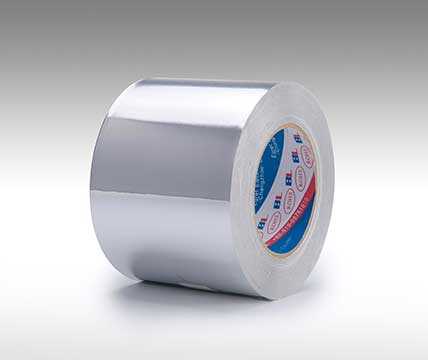
ALUMINUM FOIL TAPE
#bopp# tape #material <br>ALUMINUM FOIL TAPE <br>Egret electronics aluminum foil tape is our main & strongest products. Our aluminum tape for sale occupies 50% of all our adhesive tape business. We sell wholesale aluminum foil adhesive tape about 30 million square meters per year. We offer affordable aluminium foil tape price. Important to realize, aluminum foil tape have many types, such as pure aluminum foil tape, reinforced aluminum foil tape, fsk aluminum foil tape, alu glass cloth tape, and butyl foil tape, etc. Take pure aluminium process tape as an example, it can be with paper liner and without liner. Coated with acrylic adhesive, rubber or hot melt adhesive, according to customers different requirement on adhesion strength. It has huge demand in refrigerator industries, ideal for fixing condenser cooling tubes, maximize the cooling efficiency. Plus, it is also very popular used in ducting works, for sealing the seams of duct board as vapor barrier. Contact us and buy aluminium foil tape now! <br> <br>Aluminum Foil Tape For Sale <br>Egret aluminum foil tape has many types. For instance, pure aluminum foil tape, base material is pure aluminum, coated with glue, and paper silicon liner or without liner. Besides, pure aluminum can also laminate plastic film such as BOPP film, which is called laminated aluminum foil tape. Moreover, pure aluminum can also be reinforced by fiber mesh, etc. <br> <br>Advantages of Aluminum Foil Tape <br>light weight, it has much lighter weight compared to most of metals like iron, steel, etc. which makes the industrial adhesive tape easier transport and labor use <br> <br>flexibility, aluminum foil tape is very soft and flexible, it makes itself conforms well to contours and irregular surfaces and bonds to most substrates <br> <br>high hear and cooling conductivity, the convective heat transfer coefficient can be up to 257 W(mk),very suitable for attaching condenser cooling tubes of refrigerators. <br> <br>high moisture resistance, it provides an effective barrier to moisture, air, corrosion, can seal most of ducting seam. Act as a vapor barrier on reinforced fiberglass duct. <br> <br>The Modern Aluminum Foil Tape Manufacturing Method <br>Egret aluminum foil tape is our main & strongest products. We do the 90% manufacturing process from material to finished products. <br>Firstly, we buy high quality aluminum foil jumbos from aluminum manufacturers. <br> <br>Secondly, we formulate and mix the chemical contents to different glues, such as solvent acrylic, water-based acrylic, natural rubber or hot melt. <br> <br>Thirdly, we coat the glue on the aluminum foil by using our automatic coating lines. If no liner aluminum foil tape, we will also coat silicon on the other side. If with liner, then we directly laminate the paper liner on which. <br> <br>Sometimes, our customer might just buy the jumbo rolls. But sometimes, our customers might buy cut rolls, then we use our slitting machines to cut jumbo to small rolls. <br>[a]https%3A%2F%2Fwww.egretmfg.com%2Fproducts%2Faluminum-foil-tape%2F[/a]
Products
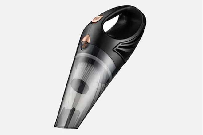
Consumer Electronics <br>Maple Sourcing excels in sourcing consumer electronics and buying directly from China. We ensure you get high-quality, innovative products that meet international standards, overcoming any cultural or legal barriers. <br> <br>Beauty & Healthcare <br>Our beauty and healthcare sourcing service provides access to top-quality, safe, and effective profitable items to import from China. We handle all complexities, ensuring your products meet all regulatory standards. <br> <br>Household Goods <br>Maple Sourcing simplifies the process of sourcing household goods from China. We guarantee quality and compliance, helping you source a wide range of durable and stylish innovative products from China. <br> <br>Tools & Hardware <br>We specialize in ecommerce sourcing tools and hardware from China. Our team ensures you receive durable, high-performance products made in China that meet your specifications and quality expectations. <br> <br>For more information about best China products to import and how to source from China, please feel free to contact us! <br> <br>If you are looking for a reliable sourcing agency, don't hesitate to contact us! <br>#customized#products#from#China <br>[a]https%3A%2F%2Fwww.maplesourcing.com%2Fsourcing-products-from-china%2F[/a]
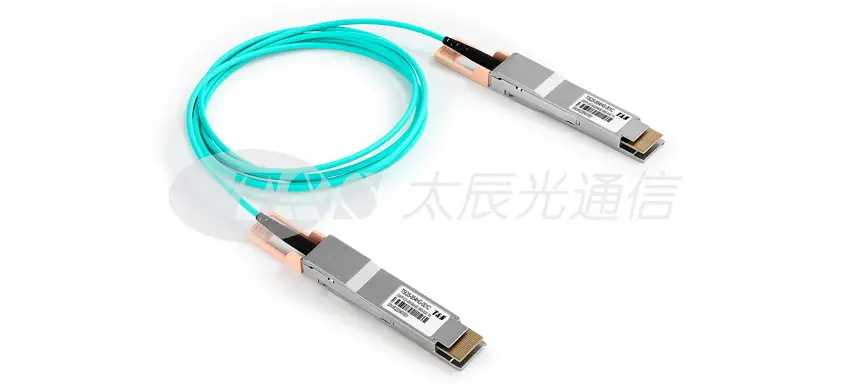
What Is QSFP+ AOC? What Are the Categories?
[a]https%3A%2F%2Fwww.china-tscom.com%2Fwhat-is-qsfp-aoc-what-are-the-categories.html[/a] <br>#optical #fiber <br>Aactive optical cable (AOC) has many advantages such as high transmission rate, long transmission distance, low energy consumption, and convenient use. It can replace passive optical cables or copper wire-based cable systems to be applied in high-density and high-bandwidth situations and has become the ideal transmission cables for data centers, consumer electronics and other fields. <br> <br>However, active optical cables can be classified into various types according to different specifications and speeds, such as 200G QSFP-DD AOC, 100G/50G QSFP28 AOC, 56G/40G QSFP AOC, SFP28 AOC, and so on. So, what are their characteristics and what are their categories? This article will give a detailed introduction to QSFP+ AOC and its categories. <br> <br>1. What is QSFP+ AOC? <br>AOC QSFP+ is an efficient integrated cable assembly product designed for short-distance multi-channel data communication and interconnection applications. Its communication distance ranges from 1 to 100 meters and it is suitable for supercomputers and SDR, DDR, QDR and other applications based on InfiniBand standards. Moreover, active optical cables have more significant advantages over interconnected copper cables, such as lower transmission power on system links, only one-fourth of the weight of direct-connected copper cables, slightly half the volume of copper cables, better air flow and heat dissipation in the cabling system of the computer room, smaller bending radius, longer transmission distance, and lower bit error rate of the product transmission performance. <br> <br>2. What are the categories of QSFP+ AOC? <br>(1) 56G QSFP+ AOC <br>56G QSFP+ AOC: QSFP+ FDR active optical cable has a built-in 850nm VCSEL laser, PIN array, integrated driver and receiver chip. It supports the standards including InfiniBand FDR, 10G Ethernet, SAS2.0 and SAS3.0, 8G and 10G fibre channel. The transmission distance of OM3 optical fiber is 100 meters, and that of OM4 optical fiber is 150 meters. It is 100% perfectly compatible with a full range of brand servers, switches, routers, PDH/SDH transmission equipment, EPON, GPON, 10G EPON, 10G GPON and WDM PON base stations. <br> <br>Its product features are as follows: <br> <br>Full-duplex 4-channel 850nm active optical cable; transmission data rate of 14.0625gbit/s/channel; set trigger SFF-8436 QSFP+ compatible; hot-swappable electrical interface; 4-channel 850nm VCSEL array; 4-channel PIN photodetector array; OM3 multimode fiber (MMF) with a maximum link length of 100m and OM4 MMF of 150 meters; low-power shell and connector; 0°C + 70°C working temperature; 3.3 V power supply voltage; RoHS6. <br> <br>(2) 40G QSFP+ to 4X10G SFP+ AOC <br>40GQSFP+ to 4X10G SFP+ AOC provides IT professionals with cost-effective host adapters, switches, and servers enabled by combining 40G QSFP and 10G SFP+. <br> <br>For typical applications, users can install this breakout active optical cable between the QSFP ports on their 40Gbps rated switches and provide four upstream 10 gb/s-sfp+ enabled switches. <br> <br>Each QSFP-SFP+ split active optical cable is characterized by a QSFP connector (sff-8436) at one end and SFP+ connector (SFF-8431), which are rated 40Gbps (SFF-8436), which is 10gb/s respectively. <br> <br>The product features are as follows: <br>The electrical interface is compatible with QSFP+ connector (setting trigger-8436) and SFP+ connector (setting trigger-8431); hot pluggable; 850nm VCSEL transmitter, PIN laser detector; OM3 MMF up to 100m; operating temperature: 0-70℃; excellent EMI performance of all metal shell; RoHS6 (lead-free). <br> <br>(3) 40G QSFP+ AOC <br>40G QSFP+AOC is the core component to realize parallel optical interconnection. It consists of ribbon fiber jumpers connected to two high-speed 40G parallel connectors. Each signal direction has 4 data channels, and each channel can work at the speed of 10Gbps. Its transmission distance is generally 1 to 100m. <br> <br>Advantages of 40G QSFP+ AOC: <br> <br>Compared with traditional 40G copper cables, 40G active optical cables have incomparable advantages: high transmission efficiency, small size, light weight, and low energy consumption; <br> <br>Compared with the optical transceiver, the AOC has no cleaning problem when the connector fails, and there is no need to test the terminal plug, which can help users save more time; <br> <br>AOC QSFP has better cabling consistency and repeatability. The closed ends are easier to avoid the influence of environment and vibration. If there is a failure, it can be replaced directly, saving costs; <br> <br>AOC is generally cheaper than optical transceivers. It can save deployment costs, and the transmission distance can also meet the requirements of a variety of short-distance transmission applications. <br>If you are looking for a reliable optical fiber manufacturer, don't hesitate to contact us!
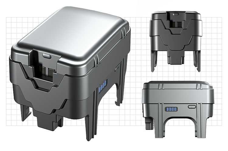
The Role of GPS Tracker Power Banks in Secure Charging
#gps #tracker #supplier <br>In the ever-evolving landscape of correctional facilities, technology is playing a crucial role in reshaping the lives of inmates. One such innovation making waves is the integration of GPS tracker power banks into the secure charging systems within prison walls. In this blog post, we will explore how these devices are empowering inmates, providing a unique blend of connectivity and security. <br> <br>Enhancing Inmate Connectivity with GPS Tracking Technology <br> <br>Incarceration often means limited access to the outside world, but GPS tracker power banks are changing the game. These devices not only serve as power sources for inmate electronics but also incorporate GPS tracking technology. This dual functionality allows correctional facilities to monitor the location of devices while giving inmates a means to stay connected with loved ones in a controlled and secure manner. <br> <br>Ensuring Secure Charging Environments <br> <br>Security is paramount within correctional facilities, and the charging of electronic devices is no exception. GPS tracker power banks are designed to provide a secure charging environment, reducing the risk of unauthorized access to inmates' devices. With features such as tamper-resistant designs and controlled charging stations, these power banks contribute to maintaining a safe and controlled atmosphere within prison walls. <br> <br>Facilitating Inmate Rehabilitation through Controlled Connectivity <br> <br>Inmate rehabilitation is a key focus of modern correctional systems, and technology plays a vital role in this process. GPS tracker power banks facilitate controlled connectivity, allowing inmates access to educational materials, vocational training apps, and other rehabilitation resources. This controlled access not only aids in skill development but also contributes to reducing recidivism by preparing inmates for a successful reintegration into society. <br> <br>Addressing Security Concerns with GPS-Integrated Power Banks <br> <br>Security concerns in correctional facilities often revolve around contraband and unauthorized communication. GPS tracker power banks address these concerns by providing a tool that combines secure charging with location tracking. This integrated approach aids prison staff in preventing the misuse of electronic devices while ensuring that inmates can responsibly use technology as part of their rehabilitation journey. <br> <br>The Future of Inmate Empowerment: Adapting to Changing Technological Landscapes <br> <br>As technology continues to advance, the role of GPS tracker power banks in inmate empowerment is expected to evolve. Future enhancements may include improved battery capacities, real-time tracking features, and even more secure charging protocols. <br> <br>In conclusion, the integration of GPS tracker power banks in secure charging systems is transforming the inmate experience within correctional facilities. By providing controlled connectivity, enhancing security, and contributing to inmate rehabilitation, these devices are indeed empowering inmates in ways that extend beyond traditional notions of incarceration. The journey towards a more connected and rehabilitative correctional system has taken a significant step forward with the adoption of GPS tracker power banks. <br> <br>As one of the gps tracking device manufacturers, We provide corrections inmate locator, sexoffender tracker, house arrest gps monitoring, inmate tracker, etc. For more information, please feel free to contact us! <br> <br>[a]https%3A%2F%2Fwww.gosafesolution.com%2Fgosafe-gps-tracker-for-domestic-violence%2F[/a]

Industrial Laminating Adhesive
#industrial <br>[a]https%3A%2F%2Fwww.adhesive4laminating.com%2Fproducts%2Findustrial-laminating-adhesive%2F[/a] <br> <br>Industrial Laminating Adhesive <br>Now many industries use the lamination technology, so the industrial laminating adhesive is used more and more in new areas like Refective Materials, Functional Fabric, Cable Wrapping, Vacuum Insulation Panel, Electronics Materials (RFID), and so on. As one of the trustworthy industrial laminating adhesive manufacturers in China, Comens provides special product that can meet the rigorous requirements to achieve excellent properties. <br> <br>Industrial Laminating Adhesive Types <br>REFLECTIVE MATERIALS ADHESIVE <br>High quality wood pulp and cellulose paper with customized processing products to ensure safety and excellent performance. <br> <br>FABRIC LAMINATION ADHESIVE <br>One component PUR type industrial laminating adhesive for fabric/film and fabric/fabric lamination, to make functional cloths with excellent waterproof and windproof. <br> <br>CABLE WRAPPING MYLAR ADHESIVE <br>This industrial laminating adhesive is designed for securing Mylar films around cables, providing excellent insulation, mechanical protection, and resistance to moisture and chemicals. <br> <br>VACUUM INSULATION PANEL ADHESIVE <br>Specifically formulated for bonding vacuum insulation panels, this industrial laminating adhesive ensures airtight sealing and thermal efficiency, crucial for energy-saving applications in construction and appliance manufacturing. <br> <br>ELECTRONICS MATERIALS (RFID) ADHESIVE <br>Used in the assembly of RFID (Radio-Frequency Identification) tags and devices, this industrial laminating adhesive offers strong bonding, durability, and reliable performance in various environmental conditions, essential for tracking and data transmission applications. <br> <br>How Does Industrial Laminating Adhesive Work? <br>Industrial laminating adhesives are specialized materials used to bond multiple layers of substrates together to form a composite material with enhanced properties such as strength, durability, and resistance to environmental factors. These industrial laminating adhesives are widely used in various industries, including automotive, aerospace, electronics, packaging, and construction, for applications ranging from laminating large panels to bonding thin films. <br> <br>The working mechanism of industrial laminating adhesives involves several key steps: <br> <br>1. Surface Preparation <br>Before applying the industrial laminating adhesive including fabric laminating adhesive, the surfaces to be laminated must be properly prepared. This can involve cleaning, drying, and sometimes roughening the surfaces to improve adhesion. Proper surface preparation ensures that the industrial laminating adhesive can form a strong bond with the substrates. <br> <br>2. Adhesive Application <br>The industrial laminating adhesive is then applied to one or both surfaces to be laminated. The method of application can vary depending on the type of adhesive and the specific requirements of the application. Common methods include spraying, rolling, brushing, and slot-die coating. <br> <br>3. Bond Formation <br>Once the industrial laminating adhesive is applied, the substrates are brought together under pressure to ensure good contact between the industrial laminating adhesive and the surfaces. The pressure applied helps to spread the adhesive evenly and remove any air bubbles trapped in the bond line. <br> <br>4. Curing <br>The adhesive then undergoes a curing process, where it transitions from a liquid or semi-liquid state to a solid state, forming a strong bond between the substrates. The curing process can be initiated or accelerated by heat, UV light, moisture, or simply by the passage of time, depending on the type of adhesive used. <br> <br>Industrial Laminating Adhesive FAQs <br>Q <br>What are industrial laminating adhesives used for? <br> <br>A <br>Industrial laminating adhesives are used to bond multiple layers of materials together in various industries. Common applications include the production of composite materials for automotive parts, aerospace components, electronic devices, packaging materials, and construction panels. <br> <br>Q <br>What types of materials can be bonded with industrial laminating adhesives? <br> <br>A <br>These industrial laminating adhesives can bond a wide range of materials, including metals, plastics, rubbers, textiles, paper, and wood. The specific type of adhesive used depends on the materials to be bonded and the required bond strength and durability. <br> <br>Q <br>How do I choose the right industrial laminating adhesive for my application? <br> <br>A <br>The choice of industrial laminating adhesive depends on several factors, including: <br> <br>The materials to be bonded <br> <br>The environmental conditions (temperature, humidity, exposure to chemicals) the bond will face <br> <br>The mechanical stresses (tension, compression, shear) the bond will need to withstand <br> <br>Regulatory and safety requirements Consulting with lamination adhesive manufacturers or suppliers can help in selecting the most suitable industrial laminating adhesive for your application. <br> <br>Q <br>Are there any environmental or health concerns associated with using industrial laminating adhesives? <br> <br>A <br>Yes, some industrial laminating adhesives, especially solvent-based and certain reactive adhesives, can release volatile organic compounds (VOCs) or other hazardous substances during application and curing. It’s important to use appropriate personal protective equipment (PPE) and ensure adequate ventilation. Water-based and hot melt adhesives are generally considered more environmentally friendly and safer to use.

Onsite Recycling Services In St Petersburg
OCM Recycle, your trusted partner for onsite electronics recycling services in St. Petersburg. We specialize in convenient and environmentally responsible disposal solutions. Ensure compliance and contribute to sustainability with our expert services. <br>[a]https%3A%2F%2Focmrecycle.com%2Fst-petersburg%2F[/a]
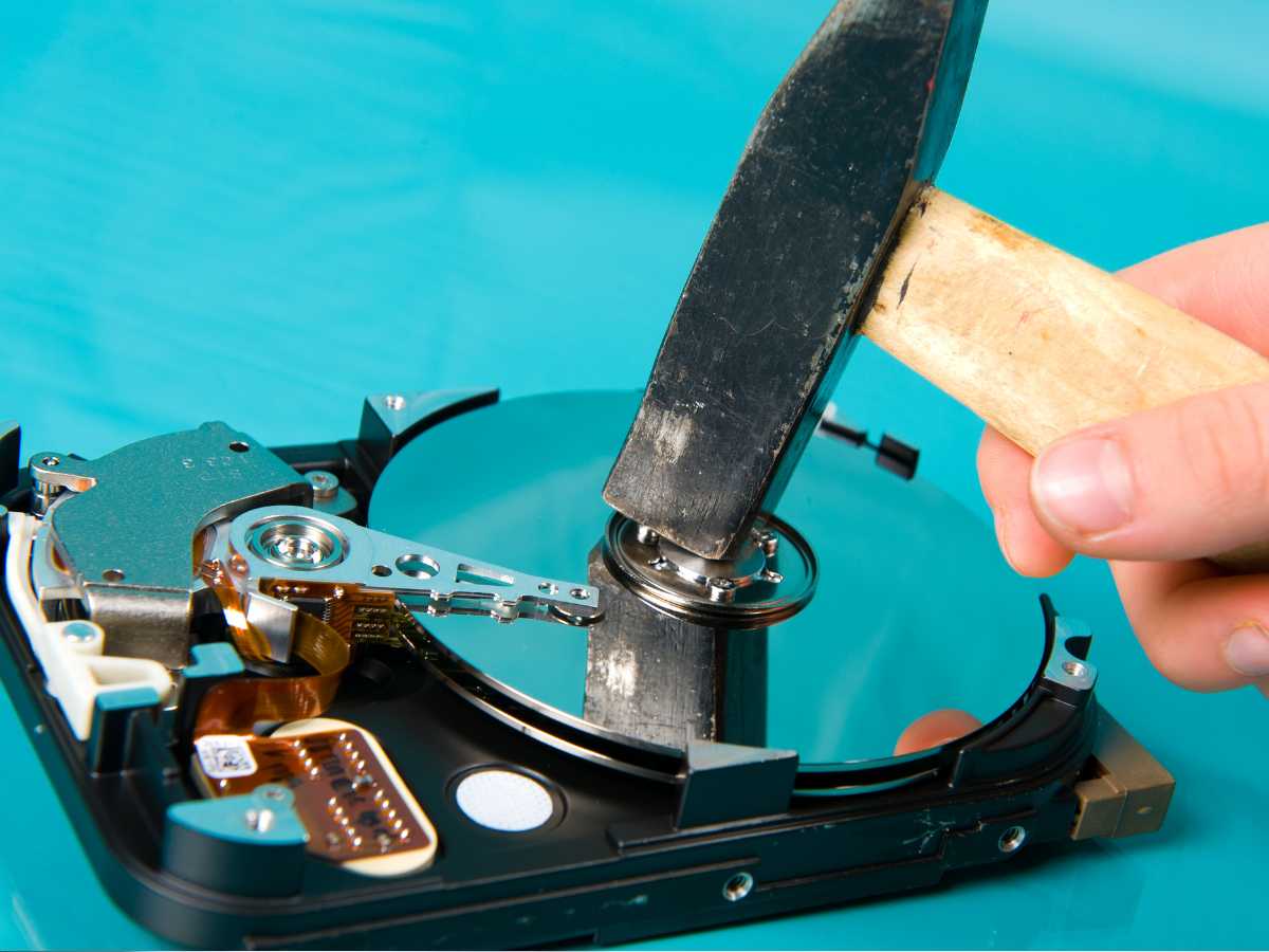
Data Destruction Services In Tampa FL
OCM Recycle offers expert electronics recycling and secure data destruction services in Tampa, FL. Partner with us to ensure your sensitive information is safely handled and compliantly disposed of. Join our commitment to sustainable practices and a greener future. <br>[a]https%3A%2F%2Focmrecycle.com%2Ftampa-fl%2F[/a]
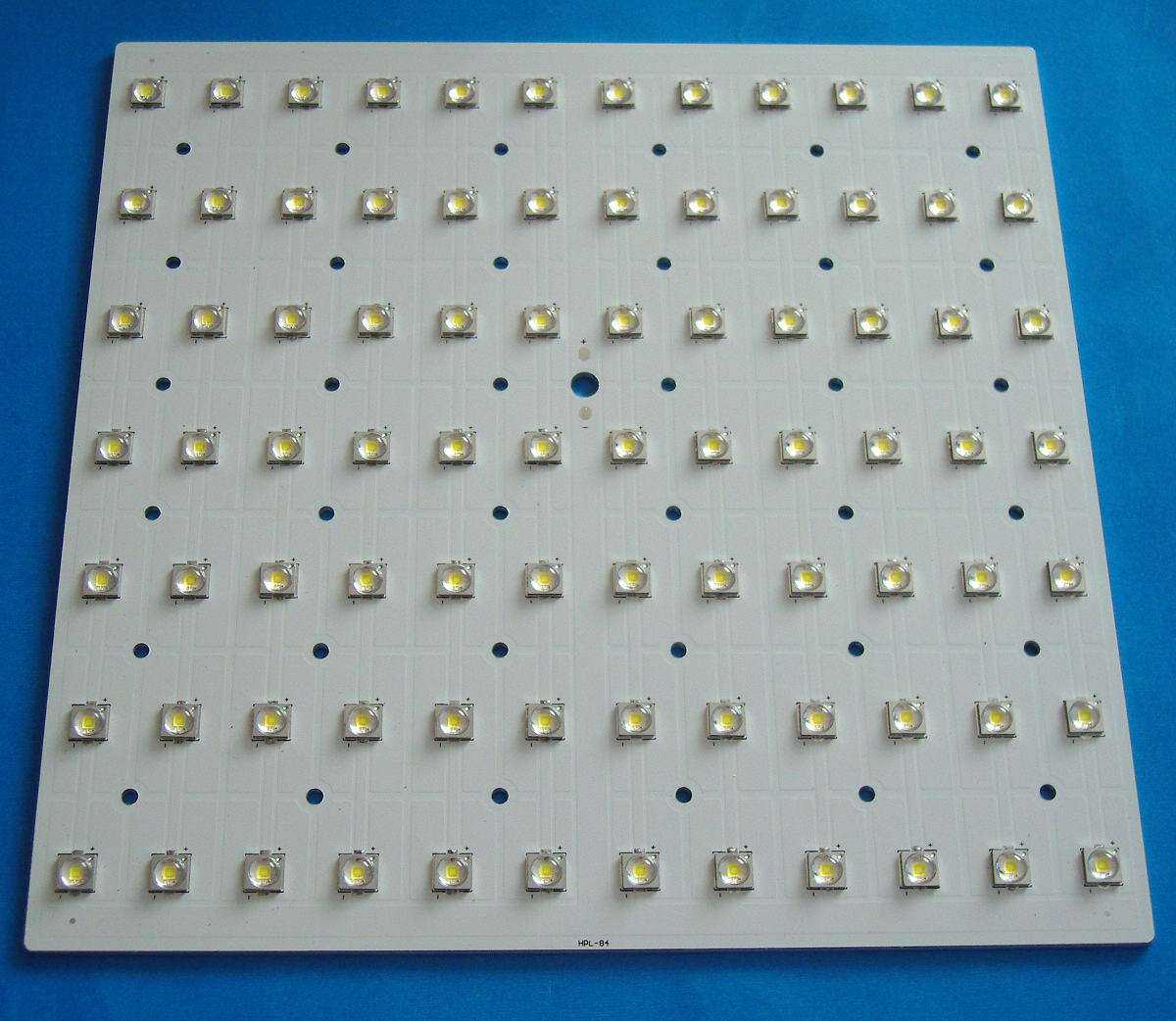
Top 1 LED PCB Board Manufacturing in China
Aluminium LED PCB Board manufacturing <br> <br> <br> <br>Aluminum PCB, or Aluminium PCB, also called Alu PCB, is one of Insulated Metal Substrate (IMS) PCBs, and is also one of the most commonly used Metal Core PCBs (MCPCB) nowadays. HitechPCB manufactures Aluminum printed circuit boards (PCB) with a full selection of high-performance substrates, and we work to be the best aluminum PCB manufacturer and provider no matter you need prototypes or high-volume production quantities. Aluminum PCBs typically are single-sided, but also can be double-sided as well. While, multilayer Aluminum PCBs are highly difficult to manufacture. <br> <br> <br> <br>LED PCB Board <br> <br>Thermal conductivity and thermal resistance of Aluminum LED PCB <br> <br> <br> <br>As a widely used electronic component Aluminum LED PCB's thermal conductivity and thermal resistance are of great significance. The thermal conductivity of led Aluminum LED PCB is the quantity describing the conductor's ability to conduct heat, which can reflect the material's ability to conduct heat. Thermal resistance refers to the change rate of the temperature difference between the two surfaces during the heat conduction process of the surface of the object. In the design and application of electronic components, the thermal conductivity and thermal resistance of led Aluminum LED PCB play a decisive role. <br> <br>Due to the different structure and composition of led Aluminum LED PCB, its thermal conductivity and thermal resistance will be different. Generally speaking, the greater the thermal conductivity of the led Aluminum LED PCB, the stronger the heat conductivity of the surface; And the smaller the thermal resistance, the smaller the temperature difference between the two surfaces. To sum up, the thermal conductivity and thermal resistance of led Aluminum LED PCB are very important parameters, which can affect the performance and service life of electronic components. <br> <br>For different application requirements, the thermal conductivity and thermal resistance of led Aluminum LED PCB will be different. For example, in high temperature environments, Aluminum LED PCB with low thermal resistance and high thermal conductivity should be used; On the contrary, if it is in a low temperature environment, the Aluminum LED PCB with large thermal resistance and small thermal conductivity should be selected. Therefore, in the process of design and application, the thermal conductivity and thermal resistance of Aluminum LED PCB should be selected scientifically and reasonably according to the actual use environment and demand, so as to obtain better use effect. Hitech can provide a wide range of aluminum-based LED PCBS to suit customer requirements. <br> <br> <br> <br>The relationship between insulating layer thickness and pressure resistance of Aluminum LED PCB <br> <br> <br> <br>Aluminum LED PCB is a kind of basic material widely used in the field of electronics. The selection and thickness of insulating layer must be considered in the production process. Insulation layer is an important part of Aluminum LED PCB, its role is to prevent short circuit and leakage between different components on the circuit board, so as to ensure the normal operation of the entire circuit. The thickness of insulation layer is very important to the performance of Aluminum LED PCB and is closely related to the voltage it can withstand. <br> <br>In general, the thicker the insulating layer of Aluminum LED PCB, the higher the voltage it can withstand. Because the thicker the insulation, the better you can isolate the different components on the board, reducing the possibility of short circuits and leakage. In addition, the thickness of the insulation layer can also affect the durability and stability of the Aluminum LED PCB, making it more durable and reliable. <br> <br>However, too thick insulation can also bring unnecessary costs and manufacturing difficulties. Therefore, factors such as cost, reliability and performance must be considered comprehensively when selecting insulation layer thickness. Generally, the insulating layer thickness of Aluminum LED PCB should be between 5mil and 10mil, but can be adjusted for specific application requirements. For higher voltage requirements, a thicker insulation layer should be selected to ensure the stability and safety of the circuit board. <br> <br>In summary, the insulating layer thickness of Aluminum LED PCB is closely related to its pressure resistance. Choosing the appropriate insulating layer thickness can improve the safety, stability and reliability of Aluminum LED PCB, so as to ensure the normal operation of the entire circuit. However, in the process of production, it is necessary to consider cost and performance factors to choose the most appropriate insulation layer thickness. <br> <br> <br> <br>Aluminium LED PCB <br> <br>Thermal expansion of Aluminum LED PCB <br> <br> <br> <br>Aluminum LED PCB is a unique metal substrate covered with copper substrate, it has good thermal conductivity, heat dissipation, electrical insulation and mechanical properties. Now let's talk about some properties of Aluminum LED PCB: <br> <br>a. Thermal expansion of Aluminum LED PCB: <br> <br>Thermal expansion and cold contraction is the common nature of substances, and the thermal expansion coefficient of different substances is different. Aluminum LED PCB can effectively solve the problem of heat dissipation, so as to alleviate the problem of thermal expansion and cold contraction of components on PCB board, and improve the durability and reliability of the whole machine and electronic equipment. In particular, the problem of hot expansion and cold contraction of SMT technology is solved. <br> <br>b, heat dissipation: <br> <br>At present, for many PCB boards with high density and power of double panels and multilayer boards, heat emission has become the most common difficulty. For example, FR4 and CEM3 are bad conductors of heat, interlayer insulation, and heat emission cannot go out. Local heating of electronic equipment cannot be excluded, leading to high temperature failure of electronic components. Thus it is widely used in high-power electronics, automobile electronic control, new energy savings, 5G communication products. <br> <br>c, the ruler of Aluminum LED PCB is relatively stable, obviously the size is much more stable than that of the printed board of insulating materials. Aluminum LED PCB and aluminum sandwich board, from 30 degrees Celsius to 140~150 degrees Celsius C heating, the size change is 2.5~3.0%. <br> <br>d, with shielding effect, instead of brittle ceramic substrate, safe use of surface mounting technology, reduce the real effective area of PCB board, replace the radiator and other components, improve the heat resistance and physical properties of the product; Reduce production costs and labor costs, <br> <br>e. Structure: 1) a. aluminum base material, the use of LF, L4M, Ly12 aluminum, the expansion strength of 30kaf/mm2, elongation of 5%. Aluminum substrate is divided into 1.01.6, 2.0, 3.2mm 4 kinds, Aluminum models 6061T6 or 5052H34• Panasonic Electric, Sumitomo R-0710, R-0771, AL C-1401ALC-1370 and other models are aluminum base copper clad plate, the current thickness of aluminum base is 1.0~6.0mm. 2) insulation, usually 50~200um• If too thick, Can play the role of insulation, prevent and metal base short circuit effect is good, but will affect the heat dissipation if too thin, can be good heat dissipation, but easy to cause the metal core and component lead short circuit • Insulation layer (or semi-cured sheet), placed on the anodized, insulated aluminum plate, after laminating with the surface of the copper layer firmly combined together <br> <br>Aluminum plate in the production of: <br> <br>(1) aluminum oxide processing: strong oil cleaning (hydroxide) -- -- dilute acid neutralization, coarsening (aluminum plate surface to form honeycomb) -- -- oxidation (um) -- - alkali neutralization -- -- the bore is sealed by baking. Each process must ensure the quality or affect the adhesion of Aluminum LED PCB. <br> <br>(2) The entire production process is not allowed to wipe the aluminum base surface, can not touch the aluminum base, damp and other dye, otherwise affect the Aluminum LED PCB bonding on it. Hitech in the production process strictly control each process, to provide customers with high quality Aluminum LED PCB. <br> <br> <br> <br>Types of Aluminum LED PCB <br> <br> <br> <br>Aluminum base plate commonly used metal aluminum base plate mainly 1000 series, 5000 series, 6000 series. The basic characteristics of these three series of aluminum are as follows: <br> <br>(1) 1000 series on behalf of 1050, 1060, 1070, 1000 series aluminum plating, also known as pure aluminum plate. Of all series, Series 1000 contains the most is 2 layers of Aluminum LED PCB, purity can reach more than 99.00%. Because it does not contain other technical elements, the production process is relatively simple and the price is also relatively cheap. It is the most commonly used series in traditional industries. Most of the products in circulation are the 1050 and 1060 series. <br> <br>The 1000 series aluminum plate is based on the last two digits to determine the minimum aluminum content of the series. For example, the last two digits of 1050 series are 50. According to the international brand naming principle, its aluminum content must reach 99.5% or more to be qualified. In the country's aluminum alloy technical standard (GB/T3880-2006), it is also clearly stipulated that the aluminum content of 1050 should reach 99.5%. Similarly, the 1060 series aluminum plate must contain more than 99.6 percent aluminum. <br> <br>(2) 5000 series stands for 5052, 5005, 5083 and 5A05 series. 5000 series aluminum plate belongs to the more commonly used alloy aluminum plate series, the main element is magnesium, magnesium content between 3-5%, also known as aluminum magnesium alloy. It is characterized by low density, high tensile strength and high elongation. In the same area, the weight of aluminum magnesium alloy is lower than other series, <br> <br>So it is often used in aviation, such as aircraft fuel tanks. In addition, it has a wide range of applications in traditional industries. Its processing technology is continuous casting and rolling, belonging to the hot rolled aluminum plate series, so it can be used for oxidation deep processing. In our country, 5000 series aluminum plate is one of more mature aluminum plate series. <br> <br>(3) 6000 series represents 6061, mainly containing magnesium and silicon, so the advantages of 4000 series and 5000 series are concentrated. 6061 is a cold treatment aluminum forgings, suitable for corrosion resistance, oxidation resistance requirements of the occasion. It has good mach inability, excellent interface characteristics, easy coating, good processing performance. <br> <br>General characteristics of 6061: excellent interface characteristics, easy coating, high strength, good workability, strong corrosion resistance. Typical uses of 6061 aluminum: aircraft parts, camera parts, couplers, Marine parts and hardware, electronic parts and connectors, etc. <br> <br>Comprehensive consideration of the material itself texture, hardness, elongation, chemical properties, price and other factors, Aluminum LED PCB generally used 5000 series aluminum alloy 5052 aluminum plate. <br> <br> <br> <br>LED PCB Board manufacturing <br> <br>Surface treatment technology of Aluminum LED PCB <br> <br> <br> <br>After the electrical parts are inserted into the printed circuit board, they should be welded automatically. In these processes, if the material bubbling, in addition to the printed circuit board processing technology is not reasonable, but also related to the Aluminum LED PCB dip welding resistance. The poor impregnation and weld ability of Aluminum LED PCB will lead to the reduction of system quality stability and the damage of the whole components. Therefore, Aluminum LED PCB manufacturers attach great importance to the quality problem of impregnation and weld ability, which directly affects the product reputation of each manufacturer. <br> <br>Aluminum LED PCB is a composite of resin, aluminum and copper foil curing. The thermal expansion coefficient of resin and aluminum, copper foil is very different, therefore, under the action of external force and heat, the internal force distribution of the plate is not uniform. If there are water molecules and some low molecules in the pores of the plate interface, under the condition of thermal shock, it will produce greater concentrated stress. If the adhesion can not resist these internal destructive forces, it will occur on the weak interface of copper foil and substrate, or lamination and foaming between the substrate layers. <br> <br>To improve the weld resistance of Aluminum LED PCB, it is necessary to reduce the factors that will destroy the structure of various surfaces in the forming and high temperature of the plate. The improvement methods mainly include the surface treatment of copper foil and aluminum, the improvement of resin adhesive, and the control of pressure and temperature in the pressing process. Hitech circuits mainly on Aluminum LED PCB aluminum surface treatment to do some expressions. <br> <br> <br> <br>Properties of aluminium substrates and surface treatment of materials <br> <br> <br> <br>Aluminum LED PCB, is a kind of raw material, is a kind of metal base copper plate with good heat dissipation function. It is an electronic glass fiber cloth or other reinforcing materials soaked in resin, a single resin as insulating bonding layer, one or two sides covered with copper foil and made of hot pressing and made of a plate material, known as copper clad laminate Aluminum LED PCB, referred to as aluminum clad copper plate. <br> <br>(1) Excellent heat dissipation performance <br> <br>Aluminum clad copper foil plate has excellent heat dissipation performance, which is the most outstanding characteristic of this kind of plate. The PCB made from it can not only effectively prevent the working temperature rise of the components and substrate loaded on it, but also rapidly dissipate the heat generated by the power amplifier components, high-power components, large circuit power switches and other components. In addition, because of its low density and light weight (2.7g/cm³), it can prevent oxidation and has a low price. Therefore, it has become the most widely used composite plate. The saturated thermal resistance of the insulated Aluminum LED PCB is 1.10℃/W and 2.8℃/W, which greatly improves the fusing current of the copper wire. <br> <br>(2) Improve the efficiency and quality of machining <br> <br>Aluminum clad copper plate has high mechanical strength and toughness, which is much better than rigid resin clad copper plate and ceramic substrate. It can realize the manufacture of large area printed boards on metal substrates, especially suitable for mounting heavy components on such substrates. In addition, the Aluminum LED PCB also has good flatness, which can be used for hammering, riveting and other aspects of assembly processing on the substrate or bending and twisting along the non-wiring part of the PCB made of it, while the traditional resin copper clad plate can not. <br> <br>(3) High stability of size <br> <br>There is a problem of thermal expansion (dimensional stability) for all kinds of copper clad plates, especially the thermal expansion in the thickness direction of the plate (Z axis), so that the quality of metallized holes and lines is affected. The main reason is that the linear expansion coefficient of the plate is different, such as copper, and the linear expansion coefficient of epoxy glass fiber cloth substrate is 3. The linear expansion of the two is very different, easy to cause the thermal expansion of the substrate difference, resulting in copper wire and metallized hole fracture or damage. The linear expansion coefficient of the Aluminum LED PCB is between, it is much smaller than the general resin substrate, and more close to the copper linear expansion coefficient, which is conducive to ensure the quality and reliability of the printed circuit.
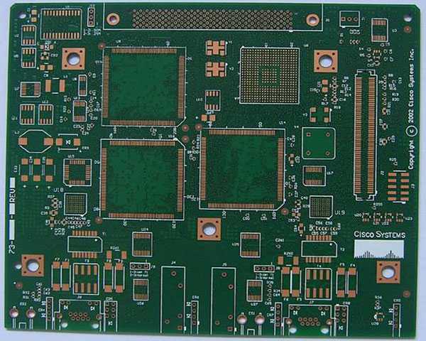
Multilayer PCB Manufacturing up to 38 Layers
Multilayer PCB Manufacturing up to 38 Layers <br>Multilayer PCB Manufacturing up to 38 layers <br> <br> <br> <br>Rigid Circuit Board Manufacturer & Assembly – One stop service PCB rigid Circuit Board is an important electronic component, support for electronic components, and a carrier for electrical connection of electronic components. Read on to learn more about multilayer PCBs, their uses and advantages in the world of modern electronics. <br> <br> <br> <br>A Multilayer Printed Circuit Board, or Multilayer PCB, is a complex circuit board composed of multiple layers of conductive material and insulating material (usually fiberglass and epoxy resin) sandwiched together. Multilayer PCB or multilayer printed circuit boards are circuit boards composed of two or more conductive layers (copper layers). The copper layer is pressed together by the resin layer (prepreg). Each layer has a conductive path or copper trace, and each layer is connected to one another through pads and vias, which act as electrical conduits. This construction allows for more complex and dense circuitry to be designed, with greater functionality and reliability compared to single- or double-sided PCBs. Multilayer PCBs are commonly used in electronic devices such as computers, smartphones, and advanced medical equipment. <br> <br> <br> <br>Multilayer PCB Prototype manufacturing <br> <br>What is Multilayer Printed Circuit Board? <br> <br> <br> <br>A Multilayer Printed Circuit Board (PCB) is a type of PCB that consists of several layers of conductive material and insulating material sandwiched together. The board is made by laminating together multiple thin layers of fiberglass or other insulating materials with copper foil. <br> <br>An integrated circuit is placed on the board, and the copper traces connected to the circuit are etched onto the inner layers of the board. The inner layers are then sandwiched together with the outer layers, forming a multilayer structure. <br> <br>Multilayer PCBs are used in high-end electronic products, such as advanced computers and mobile phones, where a high degree of density is required, and the manufacturing process is complex. They provide many benefits, including reduced size, increased reliability, and improved performance. <br> <br>Multilayer PCBs are cost-effective because they reduce the total number of components needed and improve product reliability, thus reducing the need for frequent repair services or replacement. The design flexibility of these boards also allows for more efficient use of space and improved signal routing, which aids in the performance of the product. <br> <br> <br> <br>Multilayer Printed Circuit Board stack up <br> <br> <br> <br>So what’s Multilayer PCB Benefits / Advantages? <br> <br> <br> <br>1. Increased Design Flexibility: Multilayer PCBs allow for more design flexibility and greater circuit density. With multiple layers, engineers have more space to incorporate more components and features, such as impedance control, shielding, and power planes, within the same board area. <br> <br> <br> <br>2. Increased Reliability: Multilayer PCBs are more reliable than single sided PCBs, as they are less prone to issues such as signal interference, voltage drops, and thermal stress. This is because they have a higher number of conductive layers, which allows for better shielding and more stable power distribution. <br> <br> <br> <br>3. Higher Component Density: Multilayer PCBs can accommodate a higher density of components in a smaller space while preventing signal interference. This results in a more compact and efficient design, saving manufacturers money on materials and production. <br> <br> <br> <br>4. Improved Signal Integrity: With a multilayer construction, PCBs can have better signal integrity, which means less noise and less chance of signal interference. The numerous grounds and power planes help to suppress electromagnetic interference, resulting in better connection quality. <br> <br> <br> <br>5. Better Thermal Management: Multilayer PCBs have better thermal conductivity, which reduces hot spots and improves heat dissipation. The extra layers also help to keep the heat from spreading across the board, which is important for high-power applications. <br> <br> <br> <br>6. Cost-Effective: While the initial cost of multilayer PCBs may be higher than single or double-sided PCBs, the benefits in terms of increased density, reliability, and design flexibility can mean overall cost savings in the long run. Additionally, as manufacturing techniques have evolved, the cost of producing multilayer PCBs has become more competitive. <br> <br> <br> <br>In summary, the benefits of multilayer PCBs include increased design flexibility, reliability, component density, and thermal management. They also offer improved signal integrity and can be cost-effective in the long run. These advantages make them suitable for complex electronic devices where high performance, reliability, and space-saving are required. <br> <br> <br> <br> <br> <br>-While Multilayer Printed Circuit Boards (PCBs) offer many benefits over single- or double sided PCBs, there are also some potential drawbacks to consider: <br> <br> <br> <br>1. Complexity: The multilayer PCBs are far more complex than their single-layered or double-layered counterparts. As the number of layers increases, so does complexity. This means that design and manufacturing is more challenging, which can lead to a higher cost of production. <br> <br> <br> <br>2. Cost: Multilayer PCBs are generally more expensive than single or double-layered PCBs due to their complexity. The cost of producing multilayer PCBs can increase exponentially, and the cost of manufacturing is highly dependent on the number of layers in the board, the board size, and overall complexity. <br> <br> <br> <br>3. Signal Integrity: Multilayer boards pose a higher risk of signal integrity issues due to the higher number of components and traces present in each layer. Signal interference, crosstalk, and noise can occur if proper precautions are not taken in the design process. It is therefore essential that the designer takes signal integrity into account while designing the board. <br> <br> <br> <br>4. Manufacturing Challenges: The process of cutting, etching, drilling, and laminating the multiple layers of a PCB requires highly precise equipment, which can add to the cost of manufacturing. Moreover, misalignment of layers and flaw in lamination can lead to defects that can potentially cause the PCB to stop functioning correctly. <br> <br> <br> <br>5. Environmental Impact: Multilayer PCBs contribute to electronic waste, which is a significant concern for the environment. The process of manufacturing multilayer PCBs consumes a considerable amount of energy, and the resulting waste can be toxic and difficult to recycle. <br> <br> <br> <br>Overall, Multilayer PCBs offer many advantages over single or double-sided PCBs. However, there are several issues that need to be considered during the design and manufacturing process, to achieve optimal performance. To solve your problems, here HITECH Circuits provide solutions for you. <br> <br> <br> <br>Multilayer Printed Circuit Board <br> <br> <br> <br>-Multilayer Printed Circuit Boards (PCBs) are used in a variety of applications where high performance and reliability are critical. Here are a few of the most common applications: <br> <br> <br> <br>1. Communications: Multilayer PCBs are widely used in the telecommunications industry for various applications such as cell phone base stations, satellite communications systems, and other communication devices that require high-speed data transfer rates and minimal signal loss. <br> <br> <br> <br>2. Computers: Multilayer PCBs are extensively used in computer motherboards, laptops, and other computing systems where high performance, reliability, and miniaturization are of utmost importance. <br> <br> <br> <br>3. Medical Equipment: Multilayer PCBs are a key component in many medical devices, such as imaging equipment, patient monitoring systems, and surgical instruments, where high reliability and stability are required. <br> <br> <br> <br>4. Automotive: The automotive industry uses Multilayer PCBs for applications such as engine control units, airbag systems, and lighting control systems, where reliability, durability, and efficient operation are essential. <br> <br> <br> <br>5. Aerospace and Defense: Multilayer PCBs find extensive use in aerospace and defense applications, such as missiles, satellites, and other spacecraft, where superior performance and reliability are required in extreme conditions. <br> <br> <br> <br>Overall, Multilayer PCBs are used in a wide variety of applications where increased functionality, reliability, and performance are required. With advances in technology, the use of multilayer PCBs is expected to continue to grow in the future.
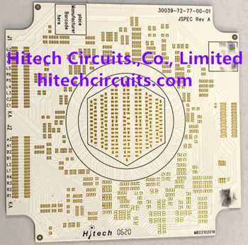
Best Ceramic PCB board, Ceramic substrate or ceramic circuit board
Ceramic PCB <br>1. What is Ceramic PCB? <br> <br> <br> <br>Ceramic PCB board is also called ceramic substrate or ceramic circuit board, ceramic copper coated plate, ceramic substrate refers to the copper foil directly bonded to alumina (Al2O3) or aluminum nitride (AlN) ceramic substrate or other ceramic substrate surface (single or double) on the special process board. The ultrathin composite substrate has excellent electrical insulation performance, high thermal conductivity, excellent soft brazing and high adhesion strength, and can be etched into a variety of graphics like PCB board, with great current-carrying capacity. Therefore, Ceramic PCB board has become the basic material of high power electronic circuit structure technology and interconnection technology. <br> <br>Ceramic PCB Manufacturing & Assembly – One-stop service The ceramic substrate (ceramic PCB) refers to a special process board in which a copper foil is directly bonded to a surface of an alumina (Al2O3 ) or aluminum nitride (AlN) ceramic substrate (single or double-sided) at a high temperature. The ultra-thin composite substrate produced has excellent electrical insulation properties, high thermal conductivity, excellent solderability, and high adhesion strength, and can etch various patterns like a PCB board, and has a large current carrying current ability. <br> <br>Ceramic PCB Circuit Board <br> <br>2. The advantages and disadvantages of Ceramic PCB <br> <br> <br> <br>(1) Ceramic PCB board has very good thermal conductivity and insulation performance. Ceramic PCB board is made of ceramic substrate, ceramic substrate itself has very good insulation and thermal conductivity, thermal conductivity of 25~230w, insulation resistivity is 10 minus 14 square, visible insulation performance is very good. <br> <br>(2) The dielectric constant of ceramic PCB board is very low, the dielectric loss is small, has very good high frequency performance, the dielectric loss of alumina ceramic PCB board is less than 0.0003@1MHz, the dielectric loss of aluminum nitride ceramic PCB board is less than 0.0005@1MHz. Low dielectric loss, high frequency performance, is widely used in the field of high frequency communication. <br> <br>(3) Ceramic PCB bonding force is strong, using bonding technology, copper foil will not fall off. <br> <br>(4) Ceramic PCB has large on-board flow, 100A current continuously passes through 1mm0.3mm thick copper body, and the temperature rises about 17℃; when 100A current continuously passes through the 2mm0.3mm thick copper body, the temperature rises only about 5℃. <br> <br>(5) Ceramic PCB board is with high temperature resistance, corrosion resistance, environmental protection, can work in a very complex environment, long-term high frequency, long service life. <br> <br>Disadvantages: fragile, scrap rate is high, this is one of the main short comings of ceramic PCB board, which leads to the production of a small area of the circuit board, the general size is less than 120mm, special custom 200mm,230mm, the general price is more expensive, the board cost is higher. In addition, because ceramic PCB board is made of ceramic material, it does not have better toughness like FR4 board, so it can make more than one meter long and wide. Another point is that the price is expensive, the requirements of electronic products are more and more rules, ceramic circuit boards are still used in some relatively high-end products, low-end products will not be used. <br> <br> <br> <br>3. Number of Ceramic PCB production layers <br> <br> <br> <br>Ceramic PCB board can do several layers at most, how many layers can be done, is a lot of customers more concerned about the topic. Ceramic PCB board can be made of multiple layers, mostly using HTCC process and LTCC process, but the processing cost is high. At present, Hitech circuit has made 4 layers, 8 layers, 16 layers of Ceramic PCB board, and so on, so far the customer feedback is good. <br> <br> <br> <br>AlN Ceramic circuit board <br> <br>4. The introduction of Ceramic PCB board <br> <br> <br> <br>Ordinary PCB is usually made of copper foil and substrate bonding, and the substrate is mostly glass fiber (FR-4), phenolic resin (FR-3) and other materials, adhesives are usually phenolic, epoxy, etc. In the process of PCB processing due to thermal stress, chemical factors, improper production technology and other reasons, or in the design process due to the two sides of the copper asymmetry, it is easy to lead to different degrees of PCB board warping. <br> <br>And another PCB substrate - ceramic substrate, due to heat dissipation performance, current carrying capacity, insulation, thermal expansion coefficient, are much better than ordinary glass fiber PCB board, so it is widely used in high-power power electronic modules, aerospace, military electronics and other products. <br> <br>Ceramic substrate and ordinary PCB using adhesive copper foil and substrate bonding together, Ceramic PCB is in the high temperature environment, through the bonding method of copper foil and ceramic substrate together, strong binding force, copper foil will not fall off, high reliability, stable performance in high temperature, high humidity environment. <br> <br> <br> <br>5. Three materials of ceramic substrate <br> <br> <br> <br>Al2O3 <br> <br>Al2O3 is the most commonly used substrate material in ceramic substrate because of its high strength and chemical stability compared to most other oxide ceramics in mechanical, thermal and electrical properties, and rich raw material sources, suitable for a variety of technical manufacturing and different shapes. According to the percentage of alumina (Al2O3) can be divided into: 75 porcelain, 96 porcelain, 99.5 porcelain. With different amounts of alumina, its electrical properties are almost unaffected, but its mechanical properties and thermal conductivity vary greatly. There is more glass in the substrate with low purity and the surface roughness is large. The higher the purity of the substrate, the cleaner, compact, the lower the dielectric loss, but the higher the price. <br> <br>BeO <br> <br>It has higher thermal conductivity than aluminum. It is applied to the occasions where high thermal conductivity is needed. It decreases rapidly after the temperature exceeds 300℃, but its toxicity limits its own development. <br> <br>AlN <br> <br>AlN are ceramics with aluminum nitride powder as the main crystalline phase. Compared with alumina ceramic substrate, the insulation resistance, insulation resistance and dielectric constant are higher. Its thermal conductivity is 7~10 times that of Al2O3, and its thermal expansion coefficient (CTE) is approximately matched with silicon wafer, which is very important for high-power semiconductor chips. In the production process, the thermal conductivity of AlN is greatly affected by the content of residual oxygen impurities, and the decrease of oxygen content can significantly improve the thermal conductivity. At present, it is no problem that the thermal conductivity of the production level reaches 170W/ (m·K). <br> <br>For the above reasons, it can be known that alumina ceramics are in a leading position in the fields of microelectronics, power electronics, hybrid microelectronics and power modules due to their superior comprehensive performance. Compared with the same size on the market (100mm×100mm×1mm), different materials of ceramic substrate price: 96% alumina 9.5 yuan, 99% alumina 18 yuan, aluminum nitride 150 yuan, beryllium oxide 650 yuan, you can see that different substrate price gap is also relatively large. <br> <br>Hitech Circuits is a professional and reliable manufacturer of Ceramic PCBs, with many years of experience in making Ceramic PCBs, which enables the manufacture of high technology, high quality and difficult performance boards, and guarantees the quality and reliability of every product delivered to customers. If you have the need to make Ceramic PCB, welcome to contact us! <br> <br> <br> <br>Alumina Ceramic PCB <br> <br> 6. Application of Ceramic PCB <br> <br> <br> <br>1. High power power electronics module, solar panel module, etc <br> <br>2. High frequency switching power supply, solid state relay <br> <br>3. Automotive electronics, aerospace, military electronics <br> <br>4. High power LED lighting products <br> <br>5. Communication antenna, automobile igniter <br> <br> <br> <br>7. Why use Ceramic PCB instead of other PCB boards? <br> <br> <br> <br>Ordinary PCB is usually made of copper foil and substrate bonding, and the substrate is mostly glass fiber (FR-4), phenolic resin (FR-3) and other materials, adhesives are usually phenolic, epoxy, etc. The main material of ceramic substrate is alumina (Al2O3), beryllium oxide (BeO), aluminum nitride (AlN) and other metal oxide ceramics, the performance of the two is quite different. <br> <br>● Plate rigidity, ordinary PCB basically belongs to chemical fiber material, its environment, temperature, processing technology and other conditions, its rigidity is far less than ceramic substrate; The latter has strong thermal stability and small coefficient of thermal expansion, which can be used in harsher environments. <br> <br>● Heat dissipation performance, ceramic substrate heat dissipation performance is excellent, very suitable for high-power device scenarios, and ordinary PCB is currently limited by material technology, far less than ceramic materials. <br> <br>● Insulation performance, good insulation of ceramic substrate, high pressure resistance, effectively protect personal safety and equipment. <br> <br>● The bonding force between ceramic substrate and copper foil is strong, the bonding technology is used, the copper foil will not fall off, which greatly improves the reliability of the plate <br> <br> <br> <br>8. What are the characteristics of Ceramic PCB <br> <br> <br> <br>● Good stability <br> <br>The surface of this plate can play a very good flame retardant effect, and good fire resistance, not easy to melt, Ceramic PCB is all acid and alkali items and other chemicals, whether it is disinfectant or cleaning agent, the surface of the Ceramic PCB will not be affected. <br> <br>● Easy to clean <br> <br>The surface of the Ceramic PCB has a strong anti-corrosion function, so it is very convenient to clean, the use of washing solution cleaning will not cause any impact on the surface and color, and the surface is very tight, no penetration, not easy to adhere to dust, but also has moisture-proof performance. <br> <br>● Beautiful <br> <br>The plate before firing, can be painted on the surface of the pattern and pattern, so fired out of the Ceramic PCB picture color is very beautiful, and not easy to be damaged, such Ceramic PCB is very beautiful and generous, and most are used for decoration. <br> <br>● Anti-static <br> <br>Ceramic PCBs are antistatic materials. <br> <br>● Resistance to scratch <br> <br>The surface structure of this kind of plate is very special, even under the action of hard objects outside, it is not easy to cause damage.
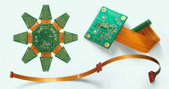
Best Flexible PCB Manufacturing
What is Flex PCB? <br> <br> <br> <br>Flexible printed circuits, also known as flex circuits, are sometimes regarded as a printed circuit board (PCB) that can bend, when in reality there are significant differences between PCB’s and flex circuits when it comes to design, fabrication and functionality. One common mistake that designers make is to design a flexible circuit using the same rules as a PCB. Flex PCB require a unique set-up and have their own set of design rules that the Hitechpcb team has termed “flex-izing” and have worked hard to perfect over the last many years. <br> <br> <br> <br>Flexible PCB, which also called Flex PCB, Flexible circuit board or flex circuit, it consists of PI base material, adhesive layer, copper layer, coverlay and sometimes with stiffeners. Flexible PCBs are now being used widely to replace traditional FR4 PCB in various different applications due to the benefits from flex PCB specially. Although more expensive than a normal rigid PCB, the right design in the right application could save weight and time in assembly, coupled with the reliability which makes flexible circuit board a worthwhile consideration. <br> <br> <br> <br>A flexible printed circuit consists of a metallic layer of traces, usually copper, bonded to a dielectric layer, usually polyimide. Thickness of the metal layer can be very thin (<.0001″) to very thick (> .010″) and the dielectric thickness can vary from .0005″ to .010″. Often an adhesive is used to bond the metal to the substrate, but other types of bonding such as vapor deposition can be used to attach the metal. <br> <br> <br> <br>flexible PCB <br> <br>How to calculate your flex pcb bend radius? <br> <br> <br> <br>Because copper tends to readily oxidize, the exposed surfaces are often covered with a protective layer, gold or solder are the two most common materials because of their conductivity and environmental durability. For non-contact areas a dielectric material is used to protect the circuitry from oxidation or electrical shorting. <br> <br> <br> <br>The number of material combinations that could go into a flexible printed circuit are nearly endless; current, capacitance, chemical and mechanical resistance, temperature extremes and type of flexing are just some of the criteria that impacts the material selections that best meet the functional needs. An experienced Hitechpcb design engineer takes the critical requirements into consideration when designing a circuit to meet your needs. <br> <br> <br> <br>Flexible printed circuit boards (FPC) has become a common component of electronic products due to its lightness and flexibility performance. It is widely used in smart terminal, wearable electronics, consumer, automotive, industrial and medical fields. The miniaturization and integrated function of electronics product development is driving FPC to fine line and multilayer design. <br> <br> <br> <br>What is Multilayer flex PCB? <br> <br>This type of flexible printed wiring boards are multilayered (with three or more conductor layers) and require plated-through holes. We could use through vias, buried vias and blind vias. <br> <br> <br> <br>A multi layer flex circuit combine several single-sided or double-sided circuits with complex interconnections, shielding and/or surface mounted technologies in a multi layer design. The multi layers may or may not be continuously laminated together throughout the production process. If your design needs require maximum flexibility, continuous lamination may not be appropriate. Multi layer circuits are an effective solution when confronted with design challenges such as: unavoidable crossovers, specific impedance requirements, elimination of crosstalk, additional shielding and high component density. You can also link here to learn more about flex pcb bending radius. <br> <br> <br> <br>Benefits to Flex PCB including: <br> <br>Assembly Error Reduction <br> <br>Decreased Assembly Time and Costs <br> <br>Design Freedom <br> <br>Flexibility during Installation <br> <br>High Density Applications <br> <br>Improved Airflow <br> <br>Increased Heat Dissipation <br> <br>Increased System Reliability <br> <br>Point-to-Point Wire Replacement <br> <br>Reliability and Durability <br> <br>Repeatable Routings <br> <br>Simplified Circuit Geometry <br> <br>Package Size and Weight Reduction <br> <br>Flex PCB Static Application <br> <br>An application where flexible circuits are flexed only to install the circuit and fit it into its application (also known as flex-to-fit or flex-to-install). A static application will typically be made using the less expensive Electro Deposited (ED) copper. <br> <br> <br> <br> <br> <br>Flex PCB Dynamic Flexing Applications <br> <br>A situation where the flexible circuit itself is dynamically (repeatedly) flexed during the actual use of the final product. Common examples include flip-type cell phones, laptops, printer heads and robotic arms. A dynamic application will require the use of Rolled Annealed (RA) copper. <br> <br> <br> <br>High Density Flex PCB Applications <br> <br>Flexible circuits allow for minutely narrow lines giving way to high density device population. Denser device populations and lighter conductors can be designed into a product, freeing space for additional product features. <br> <br> <br> <br>With a large number of investments on the facilities of flexible printed circuit board and continuously innovating the flexible circuit board manufacturing technology, Hitech Circuits is able to manufacture flexible PCBs with a great variety of technologies, from simple single sided flex PCB, double sided flex PCB to complex multilayer flexible PCB, Rigid flex pcb and support prototype FPC with laser cutting & flying probe test to mass production with toolings. <br> <br> <br> <br>Multilayer flex PCB bookbinding <br> <br>Circuit bookbinding is one of the best practices employed by Hitechpcb engineers for creating stacked PCBs. For flex PCBs, we offered a 12 layer flex PCB board with bookbinding. An additional small length is added to the circuit, making it move in an outward direction from the bend radius. There are copper traces placed at right angles to the bend. This helps restrict the circuit bend in one direction. <br> <br> <br> <br>The length to be added depends on total number of layers in the PCB, as well as the tightness of the bend. The advantage of circuit bookbinding is that it removes a great amount of tension from the various circuit layers during the bending process. The method also helps prevent buckling of the circuits at the exact bend radius. <br> <br> <br> <br>The bookbinded PCBs can easily meet the tight tolerance requirements in comparison to bonded PCBs. This is why this 12 layer flex PCB is a perfect choice for applications where stricter tolerances are required. Its polyamide construction delivers immense strength and flexibility. This flexi PCB can easily perform 180° bends. Also, the construction helps prevent buckling of inner layers, which often occurs in a long term use. This flexibility also helps reduce stress on the internal components. This 12 layer flex PCB board has better shelf life than a 12 layer bonded circuit board. The immersion gold plating offers low contact resistance, good wetting, as well as excellent shelf life. We can provide the 12 layer flex PCB board with book binding in width 4/4 mil, with minimum finish thickness 0.15 mm flex and maximum 1.6 mm. <br> <br> <br> <br>Advantages of Flexible PCB <br> <br> <br> <br>Flexible PCB technology often has a wide range of possibilities for different designs and products. <br> <br>The flexible feature is among the best attributes of the cables, wires, connectors and even PCBs. <br> <br>Some of the advantages of using the flexible circuit include: <br> <br> <br> <br>Reduces the overall weight and size. <br> <br>A flex circuit can reduce the weight of a device by up to 70%. <br> <br>Improves the packaging of electronics <br> <br>It gives you the ability to solve interconnect and packaging issues as it can bend, form and move. <br> <br>Interconnect solution as it reduces the amount of interconnects such as cables, wires, pcbs and connectors. <br> <br>Conformability as the slender nature of the material allows for making of 3D packages <br> <br>Electrical integration – You can easily come up with custom solutions basing your design on a plethora of choices of materials. Apart from that, you have the freedom to choose from the myriad of designs and plating procedures. <br> <br>Heat dissipation ability or power – The polyimide dielectric has the ability to withstand very high temperatures. You can, therefore, use it for high power applications. <br> <br>Electrical and mechanical repeatability <br> <br>Cost saving as you can save up to 30% of the total cost of hand wiring and other assembly processes. <br> <br>You can also save on space by almost 30% <br> <br>It is more reliable as it does not have any wiring errors <br> <br>Despite the numerous advantages, the flexible PCB also has its disadvantages. <br> <br>Let’s have a look. <br> <br> <br> <br>Disadvantages of Flexible PCB <br> <br>Every electronic solution must have certain demerits. <br> <br>Some of the disadvantages include: <br> <br>Flexible PCB <br> <br>A higher initial cost – Since the flex circuit is often custom for particular electronics. The initial cost of designing, photographic plate and layout is very high. This limits you to using it on large quantities to save on cost. <br> <br>Flexible circuit repairs and changes are very difficult – The initial process is not just expensive but difficult to come up with. Once you have the base map, it becomes difficult to make any more changes. Removing and replacing the covering film for repair is also extremely difficult. <br> <br>It is often small in size – The batch process of making the flexible circuits often limits the size of the flexible circuit. The production equipment limits you from making wider and longer sizes. <br> <br>Easy to damage – Improper personal operations can easily damage the flexible circuits. Rework and soldering will require the expertise of a technician. <br> <br>The process of assembly is also very difficult. <br> <br>Do not let the disadvantages kill your spirits. <br> <br> <br> <br>Why Not Make All Circuit Boards Flexible? <br> <br> <br> <br>Flexible circuit boards are certainly useful, but they are not going to replace rigid circuit boards for all applications. Cost efficiency is the main obstacle to implementing an exclusively flexible circuit board design in a consumer product. Rigid circuit boards are less expensive to manufacture and install in a typical automated high-volume fabricating facility. <br> <br> <br> <br>Typically, the ideal solution for an innovative product is one that incorporates flexible circuitry when necessary and employs solid, reliable rigid circuit boards where possible to keep manufacturing and assembly costs down. <br> <br> <br> <br>Some manufacturers even use hybrid rigid-flex printed circuit boards expressly for this purpose. This is common in laptop computers and medical devices, where rigid circuit boards can be connected to one other using ribbon-like flexible circuits. These boards can be compounded and designed to meet any number of engineering needs by focusing on the respective strengths of each circuit board base technology. <br> <br> <br> <br>Hitech Circuits creates both flexible and printed circuit boards for product manufacturers. Enjoy a consultation with one of our sales reps to find out if your product prototype design is best served by flexible or rigid circuit board types. <br> <br> <br> <br>What is Flexible PCB and Its Production Process? <br> <br> <br> <br>Flexible PCB (Flexible Printed Circuit, FPC) is very popular with excellent characteristics such as low weight and thin thickness, etc. It is also can be folded freely. Flexible PCB mainly relies on manual visual inspection with high cost and low efficiency. With the rapid development of the electronics industry, the design of printed circuit board has become more and more high -precision and high- density, traditional manual testing methods can no longer meet production needs. FPC defect automation testing has become an inevitable trend of industrial development. <br> <br>Flexible printed circuit (FPC) is a technology developed by theUnited Statesto develop aerospace rocket technology in the 1970s. It is high reliability, excellent deflection made by polyester film or polyimide as a substrate material. A flexible circuit is formed by embedding a circuit design in a thin, flexible plastic sheet that is flexible, allowing a large number of precision components to be stacked in a narrow and limited space. This circuit can be bent and folded at will. Flexible has the characteristics like light weight, small size, good heat dissipation, easy installation, etc, it breaks through the traditional interconnection technology in the structure of the flexible circuit, the material is composed of insulating film conductor and adhesive <br> <br> <br> <br>Flexible PCB includes single sided FPC, double sided FPC and multilayer FPC, etc. Single FPC has chemically etched conductive pattern layer, the conductive pattern layer on the surface of the flexible insulating substrate is calendered copper foil. The insulating substrate may be polyimide, polyethylene terephthalate, arylamide fiber ester and polyvinyl chloride. The double sided FPC on both sides of the insulating base has a conductive graphics made of etching, which increases the wiring density of the unit area. Metal hole connects the graphic connection on both sides of the insulation material to form a conductive pathway to meet the flexible design and function. The covering film can protect the single, double -sided wire and indicate the position of the component placed. According to demand, metal holes and coverage layers are optional. This type of Flexible PCB has fewer applications. Multi -layer flexible PCB is to press the single-sided or double-sided flexible circuit layer of 3 or more layers together. The metal hole is formed by drilling and electroplating, and conductive channels are formed among different layers. In this way, there is no need to use a complex welding process. Multi-layer circuits have huge functional differences in higher reliability, better thermal conductivity and more convenient assembly performance. <br> <br> <br> <br>At present, the production process of flexible PCB mainly includes looping, Sizing conductor, etching, routing of the conductors, ground planes, sizing of the holes, filleting, button plating, adhesive-backed films, screen-print liquid overcoats, photo imaginable liquid, film polymers and other processes. See the figure for the specific production process.
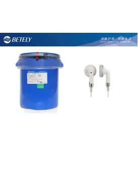
Self-adhesive Liquid Silicone Rubber For PA
[a]https%3A%2F%2Fwww.betelychina.com%2Fproducts%2Fself-adhesive-liquid-silicone-rubber-for-pa%2F[/a] <br>#liquid #silicone #rubber #material <br>Self-adhesive Liquid Fast Curing Silicone Rubber For PA <br>The self-adhesive LSR is a two-component, semitransparent self-adhesive addition liquid silicone rubber. It bonds to glass items and releases from metal molds. The LSR is easy to be released from the mold and dyeing. It has good adhesion on the PA substrate. <br> <br>Product Features Of Self-Adhesive 2 Part Liquid Silicone Rubber For PA <br>Fast curing speed <br> <br>Excellent mechanical properties <br> <br>Both injection molding and molding are available <br> <br>Application Field Of Self-Adhesive 2 Component Silicone Rubber For PA <br>It is specially suitable for those one-step molding products of PA and silicone together. Such as earphones and other electronics. <br> <br>The Performance Parameters Of Self-Adhesive Liquid Silicone Rubber For PA <br>Material/Model Unit Test Standards PA6/PA66/PPA <br> BQ-7730A/B BQ-7740A/B BQ-7750A/B BQ-7760A/B BQ-7770A/B <br>Viscosity A/B Pa·s GB/T10247 1500/3500 2000/6100 1000/2800 2500/7200 2780/10000 <br>Curing condition T10/T90 130℃/s GB/T1233 22/55 25/69 33/70 26/80 23/60 <br>Gravity g·cm-3 GB/T533 1.1 1.11 1.12 1.14 1.15 <br>Hardness TypeA GB/T531 32 40 48 61 68 <br>Tensile strength Mpa GB/T528 6.5 7 7.5 8 8 <br>Elongation % GB/T528 500 450 400 350 300 <br>Before use, please do surface treatment of metal molds (Teflon) to avoid sticking molds. <br> <br>Material/Model Unit Test Standards PA6/PA66 add 0-20%GF <br> BQ-7740A/B BQ-7750A/B BQ-7760A/B BQ-7770A/B <br>Viscosity A/B Pa·s GB/T10247 2000/6100 1000/2800 2500/7200 2780/10000 <br>Curing condition T10/T90 130℃/s GB/T1233 25/69 33/70 26/80 23/60 <br>Gravity g·cm-3 GB/T533 1.11 1.12 1.14 1.15 <br>Hardness TypeA GB/T531 40 48 61 68 <br>Tensile strength Mpa GB/T528 6.64 7.3 7.5 7.8 <br>Elongation % GB/T528 600 450 400 350 <br>Before use, please do surface treatment of metal molds (Teflon) to avoid sticking molds. <br> <br>If you want to know more about liquid silicone rubber material, please visit our website. <br> <br>As a silicone factory china, we will do our best to meet all the needs of customers.
ALUMINUM FOIL TAPE
#bopp# tape #material <br>ALUMINUM FOIL TAPE <br>Egret electronics aluminum foil tape is our main & strongest products. Our aluminum tape for sale occupies 50% of all our adhesive tape business. We sell wholesale aluminum foil adhesive tape about 30 million square meters per year. We offer affordable aluminium foil tape price. Important to realize, aluminum foil tape have many types, such as pure aluminum foil tape, reinforced aluminum foil tape, fsk aluminum foil tape, alu glass cloth tape, and butyl foil tape, etc. Take pure aluminium process tape as an example, it can be with paper liner and without liner. Coated with acrylic adhesive, rubber or hot melt adhesive, according to customers different requirement on adhesion strength. It has huge demand in refrigerator industries, ideal for fixing condenser cooling tubes, maximize the cooling efficiency. Plus, it is also very popular used in ducting works, for sealing the seams of duct board as vapor barrier. Contact us and buy aluminium foil tape now! <br> <br>Aluminum Foil Tape For Sale <br>Egret aluminum foil tape has many types. For instance, pure aluminum foil tape, base material is pure aluminum, coated with glue, and paper silicon liner or without liner. Besides, pure aluminum can also laminate plastic film such as BOPP film, which is called laminated aluminum foil tape. Moreover, pure aluminum can also be reinforced by fiber mesh, etc. <br> <br>Advantages of Aluminum Foil Tape <br>light weight, it has much lighter weight compared to most of metals like iron, steel, etc. which makes the industrial adhesive tape easier transport and labor use <br> <br>flexibility, aluminum foil tape is very soft and flexible, it makes itself conforms well to contours and irregular surfaces and bonds to most substrates <br> <br>high hear and cooling conductivity, the convective heat transfer coefficient can be up to 257 W(mk),very suitable for attaching condenser cooling tubes of refrigerators. <br> <br>high moisture resistance, it provides an effective barrier to moisture, air, corrosion, can seal most of ducting seam. Act as a vapor barrier on reinforced fiberglass duct. <br> <br>The Modern Aluminum Foil Tape Manufacturing Method <br>Egret aluminum foil tape is our main & strongest products. We do the 90% manufacturing process from material to finished products. <br>Firstly, we buy high quality aluminum foil jumbos from aluminum manufacturers. <br> <br>Secondly, we formulate and mix the chemical contents to different glues, such as solvent acrylic, water-based acrylic, natural rubber or hot melt. <br> <br>Thirdly, we coat the glue on the aluminum foil by using our automatic coating lines. If no liner aluminum foil tape, we will also coat silicon on the other side. If with liner, then we directly laminate the paper liner on which. <br> <br>Sometimes, our customer might just buy the jumbo rolls. But sometimes, our customers might buy cut rolls, then we use our slitting machines to cut jumbo to small rolls. <br>[a]https%3A%2F%2Fwww.egretmfg.com%2Fproducts%2Faluminum-foil-tape%2F[/a]
Products
Consumer Electronics <br>Maple Sourcing excels in sourcing consumer electronics and buying directly from China. We ensure you get high-quality, innovative products that meet international standards, overcoming any cultural or legal barriers. <br> <br>Beauty & Healthcare <br>Our beauty and healthcare sourcing service provides access to top-quality, safe, and effective profitable items to import from China. We handle all complexities, ensuring your products meet all regulatory standards. <br> <br>Household Goods <br>Maple Sourcing simplifies the process of sourcing household goods from China. We guarantee quality and compliance, helping you source a wide range of durable and stylish innovative products from China. <br> <br>Tools & Hardware <br>We specialize in ecommerce sourcing tools and hardware from China. Our team ensures you receive durable, high-performance products made in China that meet your specifications and quality expectations. <br> <br>For more information about best China products to import and how to source from China, please feel free to contact us! <br> <br>If you are looking for a reliable sourcing agency, don't hesitate to contact us! <br>#customized#products#from#China <br>[a]https%3A%2F%2Fwww.maplesourcing.com%2Fsourcing-products-from-china%2F[/a]
What Is QSFP+ AOC? What Are the Categories?
[a]https%3A%2F%2Fwww.china-tscom.com%2Fwhat-is-qsfp-aoc-what-are-the-categories.html[/a] <br>#optical #fiber <br>Aactive optical cable (AOC) has many advantages such as high transmission rate, long transmission distance, low energy consumption, and convenient use. It can replace passive optical cables or copper wire-based cable systems to be applied in high-density and high-bandwidth situations and has become the ideal transmission cables for data centers, consumer electronics and other fields. <br> <br>However, active optical cables can be classified into various types according to different specifications and speeds, such as 200G QSFP-DD AOC, 100G/50G QSFP28 AOC, 56G/40G QSFP AOC, SFP28 AOC, and so on. So, what are their characteristics and what are their categories? This article will give a detailed introduction to QSFP+ AOC and its categories. <br> <br>1. What is QSFP+ AOC? <br>AOC QSFP+ is an efficient integrated cable assembly product designed for short-distance multi-channel data communication and interconnection applications. Its communication distance ranges from 1 to 100 meters and it is suitable for supercomputers and SDR, DDR, QDR and other applications based on InfiniBand standards. Moreover, active optical cables have more significant advantages over interconnected copper cables, such as lower transmission power on system links, only one-fourth of the weight of direct-connected copper cables, slightly half the volume of copper cables, better air flow and heat dissipation in the cabling system of the computer room, smaller bending radius, longer transmission distance, and lower bit error rate of the product transmission performance. <br> <br>2. What are the categories of QSFP+ AOC? <br>(1) 56G QSFP+ AOC <br>56G QSFP+ AOC: QSFP+ FDR active optical cable has a built-in 850nm VCSEL laser, PIN array, integrated driver and receiver chip. It supports the standards including InfiniBand FDR, 10G Ethernet, SAS2.0 and SAS3.0, 8G and 10G fibre channel. The transmission distance of OM3 optical fiber is 100 meters, and that of OM4 optical fiber is 150 meters. It is 100% perfectly compatible with a full range of brand servers, switches, routers, PDH/SDH transmission equipment, EPON, GPON, 10G EPON, 10G GPON and WDM PON base stations. <br> <br>Its product features are as follows: <br> <br>Full-duplex 4-channel 850nm active optical cable; transmission data rate of 14.0625gbit/s/channel; set trigger SFF-8436 QSFP+ compatible; hot-swappable electrical interface; 4-channel 850nm VCSEL array; 4-channel PIN photodetector array; OM3 multimode fiber (MMF) with a maximum link length of 100m and OM4 MMF of 150 meters; low-power shell and connector; 0°C + 70°C working temperature; 3.3 V power supply voltage; RoHS6. <br> <br>(2) 40G QSFP+ to 4X10G SFP+ AOC <br>40GQSFP+ to 4X10G SFP+ AOC provides IT professionals with cost-effective host adapters, switches, and servers enabled by combining 40G QSFP and 10G SFP+. <br> <br>For typical applications, users can install this breakout active optical cable between the QSFP ports on their 40Gbps rated switches and provide four upstream 10 gb/s-sfp+ enabled switches. <br> <br>Each QSFP-SFP+ split active optical cable is characterized by a QSFP connector (sff-8436) at one end and SFP+ connector (SFF-8431), which are rated 40Gbps (SFF-8436), which is 10gb/s respectively. <br> <br>The product features are as follows: <br>The electrical interface is compatible with QSFP+ connector (setting trigger-8436) and SFP+ connector (setting trigger-8431); hot pluggable; 850nm VCSEL transmitter, PIN laser detector; OM3 MMF up to 100m; operating temperature: 0-70℃; excellent EMI performance of all metal shell; RoHS6 (lead-free). <br> <br>(3) 40G QSFP+ AOC <br>40G QSFP+AOC is the core component to realize parallel optical interconnection. It consists of ribbon fiber jumpers connected to two high-speed 40G parallel connectors. Each signal direction has 4 data channels, and each channel can work at the speed of 10Gbps. Its transmission distance is generally 1 to 100m. <br> <br>Advantages of 40G QSFP+ AOC: <br> <br>Compared with traditional 40G copper cables, 40G active optical cables have incomparable advantages: high transmission efficiency, small size, light weight, and low energy consumption; <br> <br>Compared with the optical transceiver, the AOC has no cleaning problem when the connector fails, and there is no need to test the terminal plug, which can help users save more time; <br> <br>AOC QSFP has better cabling consistency and repeatability. The closed ends are easier to avoid the influence of environment and vibration. If there is a failure, it can be replaced directly, saving costs; <br> <br>AOC is generally cheaper than optical transceivers. It can save deployment costs, and the transmission distance can also meet the requirements of a variety of short-distance transmission applications. <br>If you are looking for a reliable optical fiber manufacturer, don't hesitate to contact us!
The Role of GPS Tracker Power Banks in Secure Charging
#gps #tracker #supplier <br>In the ever-evolving landscape of correctional facilities, technology is playing a crucial role in reshaping the lives of inmates. One such innovation making waves is the integration of GPS tracker power banks into the secure charging systems within prison walls. In this blog post, we will explore how these devices are empowering inmates, providing a unique blend of connectivity and security. <br> <br>Enhancing Inmate Connectivity with GPS Tracking Technology <br> <br>Incarceration often means limited access to the outside world, but GPS tracker power banks are changing the game. These devices not only serve as power sources for inmate electronics but also incorporate GPS tracking technology. This dual functionality allows correctional facilities to monitor the location of devices while giving inmates a means to stay connected with loved ones in a controlled and secure manner. <br> <br>Ensuring Secure Charging Environments <br> <br>Security is paramount within correctional facilities, and the charging of electronic devices is no exception. GPS tracker power banks are designed to provide a secure charging environment, reducing the risk of unauthorized access to inmates' devices. With features such as tamper-resistant designs and controlled charging stations, these power banks contribute to maintaining a safe and controlled atmosphere within prison walls. <br> <br>Facilitating Inmate Rehabilitation through Controlled Connectivity <br> <br>Inmate rehabilitation is a key focus of modern correctional systems, and technology plays a vital role in this process. GPS tracker power banks facilitate controlled connectivity, allowing inmates access to educational materials, vocational training apps, and other rehabilitation resources. This controlled access not only aids in skill development but also contributes to reducing recidivism by preparing inmates for a successful reintegration into society. <br> <br>Addressing Security Concerns with GPS-Integrated Power Banks <br> <br>Security concerns in correctional facilities often revolve around contraband and unauthorized communication. GPS tracker power banks address these concerns by providing a tool that combines secure charging with location tracking. This integrated approach aids prison staff in preventing the misuse of electronic devices while ensuring that inmates can responsibly use technology as part of their rehabilitation journey. <br> <br>The Future of Inmate Empowerment: Adapting to Changing Technological Landscapes <br> <br>As technology continues to advance, the role of GPS tracker power banks in inmate empowerment is expected to evolve. Future enhancements may include improved battery capacities, real-time tracking features, and even more secure charging protocols. <br> <br>In conclusion, the integration of GPS tracker power banks in secure charging systems is transforming the inmate experience within correctional facilities. By providing controlled connectivity, enhancing security, and contributing to inmate rehabilitation, these devices are indeed empowering inmates in ways that extend beyond traditional notions of incarceration. The journey towards a more connected and rehabilitative correctional system has taken a significant step forward with the adoption of GPS tracker power banks. <br> <br>As one of the gps tracking device manufacturers, We provide corrections inmate locator, sexoffender tracker, house arrest gps monitoring, inmate tracker, etc. For more information, please feel free to contact us! <br> <br>[a]https%3A%2F%2Fwww.gosafesolution.com%2Fgosafe-gps-tracker-for-domestic-violence%2F[/a]
Industrial Laminating Adhesive
#industrial <br>[a]https%3A%2F%2Fwww.adhesive4laminating.com%2Fproducts%2Findustrial-laminating-adhesive%2F[/a] <br> <br>Industrial Laminating Adhesive <br>Now many industries use the lamination technology, so the industrial laminating adhesive is used more and more in new areas like Refective Materials, Functional Fabric, Cable Wrapping, Vacuum Insulation Panel, Electronics Materials (RFID), and so on. As one of the trustworthy industrial laminating adhesive manufacturers in China, Comens provides special product that can meet the rigorous requirements to achieve excellent properties. <br> <br>Industrial Laminating Adhesive Types <br>REFLECTIVE MATERIALS ADHESIVE <br>High quality wood pulp and cellulose paper with customized processing products to ensure safety and excellent performance. <br> <br>FABRIC LAMINATION ADHESIVE <br>One component PUR type industrial laminating adhesive for fabric/film and fabric/fabric lamination, to make functional cloths with excellent waterproof and windproof. <br> <br>CABLE WRAPPING MYLAR ADHESIVE <br>This industrial laminating adhesive is designed for securing Mylar films around cables, providing excellent insulation, mechanical protection, and resistance to moisture and chemicals. <br> <br>VACUUM INSULATION PANEL ADHESIVE <br>Specifically formulated for bonding vacuum insulation panels, this industrial laminating adhesive ensures airtight sealing and thermal efficiency, crucial for energy-saving applications in construction and appliance manufacturing. <br> <br>ELECTRONICS MATERIALS (RFID) ADHESIVE <br>Used in the assembly of RFID (Radio-Frequency Identification) tags and devices, this industrial laminating adhesive offers strong bonding, durability, and reliable performance in various environmental conditions, essential for tracking and data transmission applications. <br> <br>How Does Industrial Laminating Adhesive Work? <br>Industrial laminating adhesives are specialized materials used to bond multiple layers of substrates together to form a composite material with enhanced properties such as strength, durability, and resistance to environmental factors. These industrial laminating adhesives are widely used in various industries, including automotive, aerospace, electronics, packaging, and construction, for applications ranging from laminating large panels to bonding thin films. <br> <br>The working mechanism of industrial laminating adhesives involves several key steps: <br> <br>1. Surface Preparation <br>Before applying the industrial laminating adhesive including fabric laminating adhesive, the surfaces to be laminated must be properly prepared. This can involve cleaning, drying, and sometimes roughening the surfaces to improve adhesion. Proper surface preparation ensures that the industrial laminating adhesive can form a strong bond with the substrates. <br> <br>2. Adhesive Application <br>The industrial laminating adhesive is then applied to one or both surfaces to be laminated. The method of application can vary depending on the type of adhesive and the specific requirements of the application. Common methods include spraying, rolling, brushing, and slot-die coating. <br> <br>3. Bond Formation <br>Once the industrial laminating adhesive is applied, the substrates are brought together under pressure to ensure good contact between the industrial laminating adhesive and the surfaces. The pressure applied helps to spread the adhesive evenly and remove any air bubbles trapped in the bond line. <br> <br>4. Curing <br>The adhesive then undergoes a curing process, where it transitions from a liquid or semi-liquid state to a solid state, forming a strong bond between the substrates. The curing process can be initiated or accelerated by heat, UV light, moisture, or simply by the passage of time, depending on the type of adhesive used. <br> <br>Industrial Laminating Adhesive FAQs <br>Q <br>What are industrial laminating adhesives used for? <br> <br>A <br>Industrial laminating adhesives are used to bond multiple layers of materials together in various industries. Common applications include the production of composite materials for automotive parts, aerospace components, electronic devices, packaging materials, and construction panels. <br> <br>Q <br>What types of materials can be bonded with industrial laminating adhesives? <br> <br>A <br>These industrial laminating adhesives can bond a wide range of materials, including metals, plastics, rubbers, textiles, paper, and wood. The specific type of adhesive used depends on the materials to be bonded and the required bond strength and durability. <br> <br>Q <br>How do I choose the right industrial laminating adhesive for my application? <br> <br>A <br>The choice of industrial laminating adhesive depends on several factors, including: <br> <br>The materials to be bonded <br> <br>The environmental conditions (temperature, humidity, exposure to chemicals) the bond will face <br> <br>The mechanical stresses (tension, compression, shear) the bond will need to withstand <br> <br>Regulatory and safety requirements Consulting with lamination adhesive manufacturers or suppliers can help in selecting the most suitable industrial laminating adhesive for your application. <br> <br>Q <br>Are there any environmental or health concerns associated with using industrial laminating adhesives? <br> <br>A <br>Yes, some industrial laminating adhesives, especially solvent-based and certain reactive adhesives, can release volatile organic compounds (VOCs) or other hazardous substances during application and curing. It’s important to use appropriate personal protective equipment (PPE) and ensure adequate ventilation. Water-based and hot melt adhesives are generally considered more environmentally friendly and safer to use.
Onsite Recycling Services In St Petersburg
OCM Recycle, your trusted partner for onsite electronics recycling services in St. Petersburg. We specialize in convenient and environmentally responsible disposal solutions. Ensure compliance and contribute to sustainability with our expert services. <br>[a]https%3A%2F%2Focmrecycle.com%2Fst-petersburg%2F[/a]
Data Destruction Services In Tampa FL
OCM Recycle offers expert electronics recycling and secure data destruction services in Tampa, FL. Partner with us to ensure your sensitive information is safely handled and compliantly disposed of. Join our commitment to sustainable practices and a greener future. <br>[a]https%3A%2F%2Focmrecycle.com%2Ftampa-fl%2F[/a]
Top 1 LED PCB Board Manufacturing in China
Aluminium LED PCB Board manufacturing <br> <br> <br> <br>Aluminum PCB, or Aluminium PCB, also called Alu PCB, is one of Insulated Metal Substrate (IMS) PCBs, and is also one of the most commonly used Metal Core PCBs (MCPCB) nowadays. HitechPCB manufactures Aluminum printed circuit boards (PCB) with a full selection of high-performance substrates, and we work to be the best aluminum PCB manufacturer and provider no matter you need prototypes or high-volume production quantities. Aluminum PCBs typically are single-sided, but also can be double-sided as well. While, multilayer Aluminum PCBs are highly difficult to manufacture. <br> <br> <br> <br>LED PCB Board <br> <br>Thermal conductivity and thermal resistance of Aluminum LED PCB <br> <br> <br> <br>As a widely used electronic component Aluminum LED PCB's thermal conductivity and thermal resistance are of great significance. The thermal conductivity of led Aluminum LED PCB is the quantity describing the conductor's ability to conduct heat, which can reflect the material's ability to conduct heat. Thermal resistance refers to the change rate of the temperature difference between the two surfaces during the heat conduction process of the surface of the object. In the design and application of electronic components, the thermal conductivity and thermal resistance of led Aluminum LED PCB play a decisive role. <br> <br>Due to the different structure and composition of led Aluminum LED PCB, its thermal conductivity and thermal resistance will be different. Generally speaking, the greater the thermal conductivity of the led Aluminum LED PCB, the stronger the heat conductivity of the surface; And the smaller the thermal resistance, the smaller the temperature difference between the two surfaces. To sum up, the thermal conductivity and thermal resistance of led Aluminum LED PCB are very important parameters, which can affect the performance and service life of electronic components. <br> <br>For different application requirements, the thermal conductivity and thermal resistance of led Aluminum LED PCB will be different. For example, in high temperature environments, Aluminum LED PCB with low thermal resistance and high thermal conductivity should be used; On the contrary, if it is in a low temperature environment, the Aluminum LED PCB with large thermal resistance and small thermal conductivity should be selected. Therefore, in the process of design and application, the thermal conductivity and thermal resistance of Aluminum LED PCB should be selected scientifically and reasonably according to the actual use environment and demand, so as to obtain better use effect. Hitech can provide a wide range of aluminum-based LED PCBS to suit customer requirements. <br> <br> <br> <br>The relationship between insulating layer thickness and pressure resistance of Aluminum LED PCB <br> <br> <br> <br>Aluminum LED PCB is a kind of basic material widely used in the field of electronics. The selection and thickness of insulating layer must be considered in the production process. Insulation layer is an important part of Aluminum LED PCB, its role is to prevent short circuit and leakage between different components on the circuit board, so as to ensure the normal operation of the entire circuit. The thickness of insulation layer is very important to the performance of Aluminum LED PCB and is closely related to the voltage it can withstand. <br> <br>In general, the thicker the insulating layer of Aluminum LED PCB, the higher the voltage it can withstand. Because the thicker the insulation, the better you can isolate the different components on the board, reducing the possibility of short circuits and leakage. In addition, the thickness of the insulation layer can also affect the durability and stability of the Aluminum LED PCB, making it more durable and reliable. <br> <br>However, too thick insulation can also bring unnecessary costs and manufacturing difficulties. Therefore, factors such as cost, reliability and performance must be considered comprehensively when selecting insulation layer thickness. Generally, the insulating layer thickness of Aluminum LED PCB should be between 5mil and 10mil, but can be adjusted for specific application requirements. For higher voltage requirements, a thicker insulation layer should be selected to ensure the stability and safety of the circuit board. <br> <br>In summary, the insulating layer thickness of Aluminum LED PCB is closely related to its pressure resistance. Choosing the appropriate insulating layer thickness can improve the safety, stability and reliability of Aluminum LED PCB, so as to ensure the normal operation of the entire circuit. However, in the process of production, it is necessary to consider cost and performance factors to choose the most appropriate insulation layer thickness. <br> <br> <br> <br>Aluminium LED PCB <br> <br>Thermal expansion of Aluminum LED PCB <br> <br> <br> <br>Aluminum LED PCB is a unique metal substrate covered with copper substrate, it has good thermal conductivity, heat dissipation, electrical insulation and mechanical properties. Now let's talk about some properties of Aluminum LED PCB: <br> <br>a. Thermal expansion of Aluminum LED PCB: <br> <br>Thermal expansion and cold contraction is the common nature of substances, and the thermal expansion coefficient of different substances is different. Aluminum LED PCB can effectively solve the problem of heat dissipation, so as to alleviate the problem of thermal expansion and cold contraction of components on PCB board, and improve the durability and reliability of the whole machine and electronic equipment. In particular, the problem of hot expansion and cold contraction of SMT technology is solved. <br> <br>b, heat dissipation: <br> <br>At present, for many PCB boards with high density and power of double panels and multilayer boards, heat emission has become the most common difficulty. For example, FR4 and CEM3 are bad conductors of heat, interlayer insulation, and heat emission cannot go out. Local heating of electronic equipment cannot be excluded, leading to high temperature failure of electronic components. Thus it is widely used in high-power electronics, automobile electronic control, new energy savings, 5G communication products. <br> <br>c, the ruler of Aluminum LED PCB is relatively stable, obviously the size is much more stable than that of the printed board of insulating materials. Aluminum LED PCB and aluminum sandwich board, from 30 degrees Celsius to 140~150 degrees Celsius C heating, the size change is 2.5~3.0%. <br> <br>d, with shielding effect, instead of brittle ceramic substrate, safe use of surface mounting technology, reduce the real effective area of PCB board, replace the radiator and other components, improve the heat resistance and physical properties of the product; Reduce production costs and labor costs, <br> <br>e. Structure: 1) a. aluminum base material, the use of LF, L4M, Ly12 aluminum, the expansion strength of 30kaf/mm2, elongation of 5%. Aluminum substrate is divided into 1.01.6, 2.0, 3.2mm 4 kinds, Aluminum models 6061T6 or 5052H34• Panasonic Electric, Sumitomo R-0710, R-0771, AL C-1401ALC-1370 and other models are aluminum base copper clad plate, the current thickness of aluminum base is 1.0~6.0mm. 2) insulation, usually 50~200um• If too thick, Can play the role of insulation, prevent and metal base short circuit effect is good, but will affect the heat dissipation if too thin, can be good heat dissipation, but easy to cause the metal core and component lead short circuit • Insulation layer (or semi-cured sheet), placed on the anodized, insulated aluminum plate, after laminating with the surface of the copper layer firmly combined together <br> <br>Aluminum plate in the production of: <br> <br>(1) aluminum oxide processing: strong oil cleaning (hydroxide) -- -- dilute acid neutralization, coarsening (aluminum plate surface to form honeycomb) -- -- oxidation (um) -- - alkali neutralization -- -- the bore is sealed by baking. Each process must ensure the quality or affect the adhesion of Aluminum LED PCB. <br> <br>(2) The entire production process is not allowed to wipe the aluminum base surface, can not touch the aluminum base, damp and other dye, otherwise affect the Aluminum LED PCB bonding on it. Hitech in the production process strictly control each process, to provide customers with high quality Aluminum LED PCB. <br> <br> <br> <br>Types of Aluminum LED PCB <br> <br> <br> <br>Aluminum base plate commonly used metal aluminum base plate mainly 1000 series, 5000 series, 6000 series. The basic characteristics of these three series of aluminum are as follows: <br> <br>(1) 1000 series on behalf of 1050, 1060, 1070, 1000 series aluminum plating, also known as pure aluminum plate. Of all series, Series 1000 contains the most is 2 layers of Aluminum LED PCB, purity can reach more than 99.00%. Because it does not contain other technical elements, the production process is relatively simple and the price is also relatively cheap. It is the most commonly used series in traditional industries. Most of the products in circulation are the 1050 and 1060 series. <br> <br>The 1000 series aluminum plate is based on the last two digits to determine the minimum aluminum content of the series. For example, the last two digits of 1050 series are 50. According to the international brand naming principle, its aluminum content must reach 99.5% or more to be qualified. In the country's aluminum alloy technical standard (GB/T3880-2006), it is also clearly stipulated that the aluminum content of 1050 should reach 99.5%. Similarly, the 1060 series aluminum plate must contain more than 99.6 percent aluminum. <br> <br>(2) 5000 series stands for 5052, 5005, 5083 and 5A05 series. 5000 series aluminum plate belongs to the more commonly used alloy aluminum plate series, the main element is magnesium, magnesium content between 3-5%, also known as aluminum magnesium alloy. It is characterized by low density, high tensile strength and high elongation. In the same area, the weight of aluminum magnesium alloy is lower than other series, <br> <br>So it is often used in aviation, such as aircraft fuel tanks. In addition, it has a wide range of applications in traditional industries. Its processing technology is continuous casting and rolling, belonging to the hot rolled aluminum plate series, so it can be used for oxidation deep processing. In our country, 5000 series aluminum plate is one of more mature aluminum plate series. <br> <br>(3) 6000 series represents 6061, mainly containing magnesium and silicon, so the advantages of 4000 series and 5000 series are concentrated. 6061 is a cold treatment aluminum forgings, suitable for corrosion resistance, oxidation resistance requirements of the occasion. It has good mach inability, excellent interface characteristics, easy coating, good processing performance. <br> <br>General characteristics of 6061: excellent interface characteristics, easy coating, high strength, good workability, strong corrosion resistance. Typical uses of 6061 aluminum: aircraft parts, camera parts, couplers, Marine parts and hardware, electronic parts and connectors, etc. <br> <br>Comprehensive consideration of the material itself texture, hardness, elongation, chemical properties, price and other factors, Aluminum LED PCB generally used 5000 series aluminum alloy 5052 aluminum plate. <br> <br> <br> <br>LED PCB Board manufacturing <br> <br>Surface treatment technology of Aluminum LED PCB <br> <br> <br> <br>After the electrical parts are inserted into the printed circuit board, they should be welded automatically. In these processes, if the material bubbling, in addition to the printed circuit board processing technology is not reasonable, but also related to the Aluminum LED PCB dip welding resistance. The poor impregnation and weld ability of Aluminum LED PCB will lead to the reduction of system quality stability and the damage of the whole components. Therefore, Aluminum LED PCB manufacturers attach great importance to the quality problem of impregnation and weld ability, which directly affects the product reputation of each manufacturer. <br> <br>Aluminum LED PCB is a composite of resin, aluminum and copper foil curing. The thermal expansion coefficient of resin and aluminum, copper foil is very different, therefore, under the action of external force and heat, the internal force distribution of the plate is not uniform. If there are water molecules and some low molecules in the pores of the plate interface, under the condition of thermal shock, it will produce greater concentrated stress. If the adhesion can not resist these internal destructive forces, it will occur on the weak interface of copper foil and substrate, or lamination and foaming between the substrate layers. <br> <br>To improve the weld resistance of Aluminum LED PCB, it is necessary to reduce the factors that will destroy the structure of various surfaces in the forming and high temperature of the plate. The improvement methods mainly include the surface treatment of copper foil and aluminum, the improvement of resin adhesive, and the control of pressure and temperature in the pressing process. Hitech circuits mainly on Aluminum LED PCB aluminum surface treatment to do some expressions. <br> <br> <br> <br>Properties of aluminium substrates and surface treatment of materials <br> <br> <br> <br>Aluminum LED PCB, is a kind of raw material, is a kind of metal base copper plate with good heat dissipation function. It is an electronic glass fiber cloth or other reinforcing materials soaked in resin, a single resin as insulating bonding layer, one or two sides covered with copper foil and made of hot pressing and made of a plate material, known as copper clad laminate Aluminum LED PCB, referred to as aluminum clad copper plate. <br> <br>(1) Excellent heat dissipation performance <br> <br>Aluminum clad copper foil plate has excellent heat dissipation performance, which is the most outstanding characteristic of this kind of plate. The PCB made from it can not only effectively prevent the working temperature rise of the components and substrate loaded on it, but also rapidly dissipate the heat generated by the power amplifier components, high-power components, large circuit power switches and other components. In addition, because of its low density and light weight (2.7g/cm³), it can prevent oxidation and has a low price. Therefore, it has become the most widely used composite plate. The saturated thermal resistance of the insulated Aluminum LED PCB is 1.10℃/W and 2.8℃/W, which greatly improves the fusing current of the copper wire. <br> <br>(2) Improve the efficiency and quality of machining <br> <br>Aluminum clad copper plate has high mechanical strength and toughness, which is much better than rigid resin clad copper plate and ceramic substrate. It can realize the manufacture of large area printed boards on metal substrates, especially suitable for mounting heavy components on such substrates. In addition, the Aluminum LED PCB also has good flatness, which can be used for hammering, riveting and other aspects of assembly processing on the substrate or bending and twisting along the non-wiring part of the PCB made of it, while the traditional resin copper clad plate can not. <br> <br>(3) High stability of size <br> <br>There is a problem of thermal expansion (dimensional stability) for all kinds of copper clad plates, especially the thermal expansion in the thickness direction of the plate (Z axis), so that the quality of metallized holes and lines is affected. The main reason is that the linear expansion coefficient of the plate is different, such as copper, and the linear expansion coefficient of epoxy glass fiber cloth substrate is 3. The linear expansion of the two is very different, easy to cause the thermal expansion of the substrate difference, resulting in copper wire and metallized hole fracture or damage. The linear expansion coefficient of the Aluminum LED PCB is between, it is much smaller than the general resin substrate, and more close to the copper linear expansion coefficient, which is conducive to ensure the quality and reliability of the printed circuit.
Multilayer PCB Manufacturing up to 38 Layers
Multilayer PCB Manufacturing up to 38 Layers <br>Multilayer PCB Manufacturing up to 38 layers <br> <br> <br> <br>Rigid Circuit Board Manufacturer & Assembly – One stop service PCB rigid Circuit Board is an important electronic component, support for electronic components, and a carrier for electrical connection of electronic components. Read on to learn more about multilayer PCBs, their uses and advantages in the world of modern electronics. <br> <br> <br> <br>A Multilayer Printed Circuit Board, or Multilayer PCB, is a complex circuit board composed of multiple layers of conductive material and insulating material (usually fiberglass and epoxy resin) sandwiched together. Multilayer PCB or multilayer printed circuit boards are circuit boards composed of two or more conductive layers (copper layers). The copper layer is pressed together by the resin layer (prepreg). Each layer has a conductive path or copper trace, and each layer is connected to one another through pads and vias, which act as electrical conduits. This construction allows for more complex and dense circuitry to be designed, with greater functionality and reliability compared to single- or double-sided PCBs. Multilayer PCBs are commonly used in electronic devices such as computers, smartphones, and advanced medical equipment. <br> <br> <br> <br>Multilayer PCB Prototype manufacturing <br> <br>What is Multilayer Printed Circuit Board? <br> <br> <br> <br>A Multilayer Printed Circuit Board (PCB) is a type of PCB that consists of several layers of conductive material and insulating material sandwiched together. The board is made by laminating together multiple thin layers of fiberglass or other insulating materials with copper foil. <br> <br>An integrated circuit is placed on the board, and the copper traces connected to the circuit are etched onto the inner layers of the board. The inner layers are then sandwiched together with the outer layers, forming a multilayer structure. <br> <br>Multilayer PCBs are used in high-end electronic products, such as advanced computers and mobile phones, where a high degree of density is required, and the manufacturing process is complex. They provide many benefits, including reduced size, increased reliability, and improved performance. <br> <br>Multilayer PCBs are cost-effective because they reduce the total number of components needed and improve product reliability, thus reducing the need for frequent repair services or replacement. The design flexibility of these boards also allows for more efficient use of space and improved signal routing, which aids in the performance of the product. <br> <br> <br> <br>Multilayer Printed Circuit Board stack up <br> <br> <br> <br>So what’s Multilayer PCB Benefits / Advantages? <br> <br> <br> <br>1. Increased Design Flexibility: Multilayer PCBs allow for more design flexibility and greater circuit density. With multiple layers, engineers have more space to incorporate more components and features, such as impedance control, shielding, and power planes, within the same board area. <br> <br> <br> <br>2. Increased Reliability: Multilayer PCBs are more reliable than single sided PCBs, as they are less prone to issues such as signal interference, voltage drops, and thermal stress. This is because they have a higher number of conductive layers, which allows for better shielding and more stable power distribution. <br> <br> <br> <br>3. Higher Component Density: Multilayer PCBs can accommodate a higher density of components in a smaller space while preventing signal interference. This results in a more compact and efficient design, saving manufacturers money on materials and production. <br> <br> <br> <br>4. Improved Signal Integrity: With a multilayer construction, PCBs can have better signal integrity, which means less noise and less chance of signal interference. The numerous grounds and power planes help to suppress electromagnetic interference, resulting in better connection quality. <br> <br> <br> <br>5. Better Thermal Management: Multilayer PCBs have better thermal conductivity, which reduces hot spots and improves heat dissipation. The extra layers also help to keep the heat from spreading across the board, which is important for high-power applications. <br> <br> <br> <br>6. Cost-Effective: While the initial cost of multilayer PCBs may be higher than single or double-sided PCBs, the benefits in terms of increased density, reliability, and design flexibility can mean overall cost savings in the long run. Additionally, as manufacturing techniques have evolved, the cost of producing multilayer PCBs has become more competitive. <br> <br> <br> <br>In summary, the benefits of multilayer PCBs include increased design flexibility, reliability, component density, and thermal management. They also offer improved signal integrity and can be cost-effective in the long run. These advantages make them suitable for complex electronic devices where high performance, reliability, and space-saving are required. <br> <br> <br> <br> <br> <br>-While Multilayer Printed Circuit Boards (PCBs) offer many benefits over single- or double sided PCBs, there are also some potential drawbacks to consider: <br> <br> <br> <br>1. Complexity: The multilayer PCBs are far more complex than their single-layered or double-layered counterparts. As the number of layers increases, so does complexity. This means that design and manufacturing is more challenging, which can lead to a higher cost of production. <br> <br> <br> <br>2. Cost: Multilayer PCBs are generally more expensive than single or double-layered PCBs due to their complexity. The cost of producing multilayer PCBs can increase exponentially, and the cost of manufacturing is highly dependent on the number of layers in the board, the board size, and overall complexity. <br> <br> <br> <br>3. Signal Integrity: Multilayer boards pose a higher risk of signal integrity issues due to the higher number of components and traces present in each layer. Signal interference, crosstalk, and noise can occur if proper precautions are not taken in the design process. It is therefore essential that the designer takes signal integrity into account while designing the board. <br> <br> <br> <br>4. Manufacturing Challenges: The process of cutting, etching, drilling, and laminating the multiple layers of a PCB requires highly precise equipment, which can add to the cost of manufacturing. Moreover, misalignment of layers and flaw in lamination can lead to defects that can potentially cause the PCB to stop functioning correctly. <br> <br> <br> <br>5. Environmental Impact: Multilayer PCBs contribute to electronic waste, which is a significant concern for the environment. The process of manufacturing multilayer PCBs consumes a considerable amount of energy, and the resulting waste can be toxic and difficult to recycle. <br> <br> <br> <br>Overall, Multilayer PCBs offer many advantages over single or double-sided PCBs. However, there are several issues that need to be considered during the design and manufacturing process, to achieve optimal performance. To solve your problems, here HITECH Circuits provide solutions for you. <br> <br> <br> <br>Multilayer Printed Circuit Board <br> <br> <br> <br>-Multilayer Printed Circuit Boards (PCBs) are used in a variety of applications where high performance and reliability are critical. Here are a few of the most common applications: <br> <br> <br> <br>1. Communications: Multilayer PCBs are widely used in the telecommunications industry for various applications such as cell phone base stations, satellite communications systems, and other communication devices that require high-speed data transfer rates and minimal signal loss. <br> <br> <br> <br>2. Computers: Multilayer PCBs are extensively used in computer motherboards, laptops, and other computing systems where high performance, reliability, and miniaturization are of utmost importance. <br> <br> <br> <br>3. Medical Equipment: Multilayer PCBs are a key component in many medical devices, such as imaging equipment, patient monitoring systems, and surgical instruments, where high reliability and stability are required. <br> <br> <br> <br>4. Automotive: The automotive industry uses Multilayer PCBs for applications such as engine control units, airbag systems, and lighting control systems, where reliability, durability, and efficient operation are essential. <br> <br> <br> <br>5. Aerospace and Defense: Multilayer PCBs find extensive use in aerospace and defense applications, such as missiles, satellites, and other spacecraft, where superior performance and reliability are required in extreme conditions. <br> <br> <br> <br>Overall, Multilayer PCBs are used in a wide variety of applications where increased functionality, reliability, and performance are required. With advances in technology, the use of multilayer PCBs is expected to continue to grow in the future.
Best Ceramic PCB board, Ceramic substrate or ceramic circuit board
Ceramic PCB <br>1. What is Ceramic PCB? <br> <br> <br> <br>Ceramic PCB board is also called ceramic substrate or ceramic circuit board, ceramic copper coated plate, ceramic substrate refers to the copper foil directly bonded to alumina (Al2O3) or aluminum nitride (AlN) ceramic substrate or other ceramic substrate surface (single or double) on the special process board. The ultrathin composite substrate has excellent electrical insulation performance, high thermal conductivity, excellent soft brazing and high adhesion strength, and can be etched into a variety of graphics like PCB board, with great current-carrying capacity. Therefore, Ceramic PCB board has become the basic material of high power electronic circuit structure technology and interconnection technology. <br> <br>Ceramic PCB Manufacturing & Assembly – One-stop service The ceramic substrate (ceramic PCB) refers to a special process board in which a copper foil is directly bonded to a surface of an alumina (Al2O3 ) or aluminum nitride (AlN) ceramic substrate (single or double-sided) at a high temperature. The ultra-thin composite substrate produced has excellent electrical insulation properties, high thermal conductivity, excellent solderability, and high adhesion strength, and can etch various patterns like a PCB board, and has a large current carrying current ability. <br> <br>Ceramic PCB Circuit Board <br> <br>2. The advantages and disadvantages of Ceramic PCB <br> <br> <br> <br>(1) Ceramic PCB board has very good thermal conductivity and insulation performance. Ceramic PCB board is made of ceramic substrate, ceramic substrate itself has very good insulation and thermal conductivity, thermal conductivity of 25~230w, insulation resistivity is 10 minus 14 square, visible insulation performance is very good. <br> <br>(2) The dielectric constant of ceramic PCB board is very low, the dielectric loss is small, has very good high frequency performance, the dielectric loss of alumina ceramic PCB board is less than 0.0003@1MHz, the dielectric loss of aluminum nitride ceramic PCB board is less than 0.0005@1MHz. Low dielectric loss, high frequency performance, is widely used in the field of high frequency communication. <br> <br>(3) Ceramic PCB bonding force is strong, using bonding technology, copper foil will not fall off. <br> <br>(4) Ceramic PCB has large on-board flow, 100A current continuously passes through 1mm0.3mm thick copper body, and the temperature rises about 17℃; when 100A current continuously passes through the 2mm0.3mm thick copper body, the temperature rises only about 5℃. <br> <br>(5) Ceramic PCB board is with high temperature resistance, corrosion resistance, environmental protection, can work in a very complex environment, long-term high frequency, long service life. <br> <br>Disadvantages: fragile, scrap rate is high, this is one of the main short comings of ceramic PCB board, which leads to the production of a small area of the circuit board, the general size is less than 120mm, special custom 200mm,230mm, the general price is more expensive, the board cost is higher. In addition, because ceramic PCB board is made of ceramic material, it does not have better toughness like FR4 board, so it can make more than one meter long and wide. Another point is that the price is expensive, the requirements of electronic products are more and more rules, ceramic circuit boards are still used in some relatively high-end products, low-end products will not be used. <br> <br> <br> <br>3. Number of Ceramic PCB production layers <br> <br> <br> <br>Ceramic PCB board can do several layers at most, how many layers can be done, is a lot of customers more concerned about the topic. Ceramic PCB board can be made of multiple layers, mostly using HTCC process and LTCC process, but the processing cost is high. At present, Hitech circuit has made 4 layers, 8 layers, 16 layers of Ceramic PCB board, and so on, so far the customer feedback is good. <br> <br> <br> <br>AlN Ceramic circuit board <br> <br>4. The introduction of Ceramic PCB board <br> <br> <br> <br>Ordinary PCB is usually made of copper foil and substrate bonding, and the substrate is mostly glass fiber (FR-4), phenolic resin (FR-3) and other materials, adhesives are usually phenolic, epoxy, etc. In the process of PCB processing due to thermal stress, chemical factors, improper production technology and other reasons, or in the design process due to the two sides of the copper asymmetry, it is easy to lead to different degrees of PCB board warping. <br> <br>And another PCB substrate - ceramic substrate, due to heat dissipation performance, current carrying capacity, insulation, thermal expansion coefficient, are much better than ordinary glass fiber PCB board, so it is widely used in high-power power electronic modules, aerospace, military electronics and other products. <br> <br>Ceramic substrate and ordinary PCB using adhesive copper foil and substrate bonding together, Ceramic PCB is in the high temperature environment, through the bonding method of copper foil and ceramic substrate together, strong binding force, copper foil will not fall off, high reliability, stable performance in high temperature, high humidity environment. <br> <br> <br> <br>5. Three materials of ceramic substrate <br> <br> <br> <br>Al2O3 <br> <br>Al2O3 is the most commonly used substrate material in ceramic substrate because of its high strength and chemical stability compared to most other oxide ceramics in mechanical, thermal and electrical properties, and rich raw material sources, suitable for a variety of technical manufacturing and different shapes. According to the percentage of alumina (Al2O3) can be divided into: 75 porcelain, 96 porcelain, 99.5 porcelain. With different amounts of alumina, its electrical properties are almost unaffected, but its mechanical properties and thermal conductivity vary greatly. There is more glass in the substrate with low purity and the surface roughness is large. The higher the purity of the substrate, the cleaner, compact, the lower the dielectric loss, but the higher the price. <br> <br>BeO <br> <br>It has higher thermal conductivity than aluminum. It is applied to the occasions where high thermal conductivity is needed. It decreases rapidly after the temperature exceeds 300℃, but its toxicity limits its own development. <br> <br>AlN <br> <br>AlN are ceramics with aluminum nitride powder as the main crystalline phase. Compared with alumina ceramic substrate, the insulation resistance, insulation resistance and dielectric constant are higher. Its thermal conductivity is 7~10 times that of Al2O3, and its thermal expansion coefficient (CTE) is approximately matched with silicon wafer, which is very important for high-power semiconductor chips. In the production process, the thermal conductivity of AlN is greatly affected by the content of residual oxygen impurities, and the decrease of oxygen content can significantly improve the thermal conductivity. At present, it is no problem that the thermal conductivity of the production level reaches 170W/ (m·K). <br> <br>For the above reasons, it can be known that alumina ceramics are in a leading position in the fields of microelectronics, power electronics, hybrid microelectronics and power modules due to their superior comprehensive performance. Compared with the same size on the market (100mm×100mm×1mm), different materials of ceramic substrate price: 96% alumina 9.5 yuan, 99% alumina 18 yuan, aluminum nitride 150 yuan, beryllium oxide 650 yuan, you can see that different substrate price gap is also relatively large. <br> <br>Hitech Circuits is a professional and reliable manufacturer of Ceramic PCBs, with many years of experience in making Ceramic PCBs, which enables the manufacture of high technology, high quality and difficult performance boards, and guarantees the quality and reliability of every product delivered to customers. If you have the need to make Ceramic PCB, welcome to contact us! <br> <br> <br> <br>Alumina Ceramic PCB <br> <br> 6. Application of Ceramic PCB <br> <br> <br> <br>1. High power power electronics module, solar panel module, etc <br> <br>2. High frequency switching power supply, solid state relay <br> <br>3. Automotive electronics, aerospace, military electronics <br> <br>4. High power LED lighting products <br> <br>5. Communication antenna, automobile igniter <br> <br> <br> <br>7. Why use Ceramic PCB instead of other PCB boards? <br> <br> <br> <br>Ordinary PCB is usually made of copper foil and substrate bonding, and the substrate is mostly glass fiber (FR-4), phenolic resin (FR-3) and other materials, adhesives are usually phenolic, epoxy, etc. The main material of ceramic substrate is alumina (Al2O3), beryllium oxide (BeO), aluminum nitride (AlN) and other metal oxide ceramics, the performance of the two is quite different. <br> <br>● Plate rigidity, ordinary PCB basically belongs to chemical fiber material, its environment, temperature, processing technology and other conditions, its rigidity is far less than ceramic substrate; The latter has strong thermal stability and small coefficient of thermal expansion, which can be used in harsher environments. <br> <br>● Heat dissipation performance, ceramic substrate heat dissipation performance is excellent, very suitable for high-power device scenarios, and ordinary PCB is currently limited by material technology, far less than ceramic materials. <br> <br>● Insulation performance, good insulation of ceramic substrate, high pressure resistance, effectively protect personal safety and equipment. <br> <br>● The bonding force between ceramic substrate and copper foil is strong, the bonding technology is used, the copper foil will not fall off, which greatly improves the reliability of the plate <br> <br> <br> <br>8. What are the characteristics of Ceramic PCB <br> <br> <br> <br>● Good stability <br> <br>The surface of this plate can play a very good flame retardant effect, and good fire resistance, not easy to melt, Ceramic PCB is all acid and alkali items and other chemicals, whether it is disinfectant or cleaning agent, the surface of the Ceramic PCB will not be affected. <br> <br>● Easy to clean <br> <br>The surface of the Ceramic PCB has a strong anti-corrosion function, so it is very convenient to clean, the use of washing solution cleaning will not cause any impact on the surface and color, and the surface is very tight, no penetration, not easy to adhere to dust, but also has moisture-proof performance. <br> <br>● Beautiful <br> <br>The plate before firing, can be painted on the surface of the pattern and pattern, so fired out of the Ceramic PCB picture color is very beautiful, and not easy to be damaged, such Ceramic PCB is very beautiful and generous, and most are used for decoration. <br> <br>● Anti-static <br> <br>Ceramic PCBs are antistatic materials. <br> <br>● Resistance to scratch <br> <br>The surface structure of this kind of plate is very special, even under the action of hard objects outside, it is not easy to cause damage.
Best Flexible PCB Manufacturing
What is Flex PCB? <br> <br> <br> <br>Flexible printed circuits, also known as flex circuits, are sometimes regarded as a printed circuit board (PCB) that can bend, when in reality there are significant differences between PCB’s and flex circuits when it comes to design, fabrication and functionality. One common mistake that designers make is to design a flexible circuit using the same rules as a PCB. Flex PCB require a unique set-up and have their own set of design rules that the Hitechpcb team has termed “flex-izing” and have worked hard to perfect over the last many years. <br> <br> <br> <br>Flexible PCB, which also called Flex PCB, Flexible circuit board or flex circuit, it consists of PI base material, adhesive layer, copper layer, coverlay and sometimes with stiffeners. Flexible PCBs are now being used widely to replace traditional FR4 PCB in various different applications due to the benefits from flex PCB specially. Although more expensive than a normal rigid PCB, the right design in the right application could save weight and time in assembly, coupled with the reliability which makes flexible circuit board a worthwhile consideration. <br> <br> <br> <br>A flexible printed circuit consists of a metallic layer of traces, usually copper, bonded to a dielectric layer, usually polyimide. Thickness of the metal layer can be very thin (<.0001″) to very thick (> .010″) and the dielectric thickness can vary from .0005″ to .010″. Often an adhesive is used to bond the metal to the substrate, but other types of bonding such as vapor deposition can be used to attach the metal. <br> <br> <br> <br>flexible PCB <br> <br>How to calculate your flex pcb bend radius? <br> <br> <br> <br>Because copper tends to readily oxidize, the exposed surfaces are often covered with a protective layer, gold or solder are the two most common materials because of their conductivity and environmental durability. For non-contact areas a dielectric material is used to protect the circuitry from oxidation or electrical shorting. <br> <br> <br> <br>The number of material combinations that could go into a flexible printed circuit are nearly endless; current, capacitance, chemical and mechanical resistance, temperature extremes and type of flexing are just some of the criteria that impacts the material selections that best meet the functional needs. An experienced Hitechpcb design engineer takes the critical requirements into consideration when designing a circuit to meet your needs. <br> <br> <br> <br>Flexible printed circuit boards (FPC) has become a common component of electronic products due to its lightness and flexibility performance. It is widely used in smart terminal, wearable electronics, consumer, automotive, industrial and medical fields. The miniaturization and integrated function of electronics product development is driving FPC to fine line and multilayer design. <br> <br> <br> <br>What is Multilayer flex PCB? <br> <br>This type of flexible printed wiring boards are multilayered (with three or more conductor layers) and require plated-through holes. We could use through vias, buried vias and blind vias. <br> <br> <br> <br>A multi layer flex circuit combine several single-sided or double-sided circuits with complex interconnections, shielding and/or surface mounted technologies in a multi layer design. The multi layers may or may not be continuously laminated together throughout the production process. If your design needs require maximum flexibility, continuous lamination may not be appropriate. Multi layer circuits are an effective solution when confronted with design challenges such as: unavoidable crossovers, specific impedance requirements, elimination of crosstalk, additional shielding and high component density. You can also link here to learn more about flex pcb bending radius. <br> <br> <br> <br>Benefits to Flex PCB including: <br> <br>Assembly Error Reduction <br> <br>Decreased Assembly Time and Costs <br> <br>Design Freedom <br> <br>Flexibility during Installation <br> <br>High Density Applications <br> <br>Improved Airflow <br> <br>Increased Heat Dissipation <br> <br>Increased System Reliability <br> <br>Point-to-Point Wire Replacement <br> <br>Reliability and Durability <br> <br>Repeatable Routings <br> <br>Simplified Circuit Geometry <br> <br>Package Size and Weight Reduction <br> <br>Flex PCB Static Application <br> <br>An application where flexible circuits are flexed only to install the circuit and fit it into its application (also known as flex-to-fit or flex-to-install). A static application will typically be made using the less expensive Electro Deposited (ED) copper. <br> <br> <br> <br> <br> <br>Flex PCB Dynamic Flexing Applications <br> <br>A situation where the flexible circuit itself is dynamically (repeatedly) flexed during the actual use of the final product. Common examples include flip-type cell phones, laptops, printer heads and robotic arms. A dynamic application will require the use of Rolled Annealed (RA) copper. <br> <br> <br> <br>High Density Flex PCB Applications <br> <br>Flexible circuits allow for minutely narrow lines giving way to high density device population. Denser device populations and lighter conductors can be designed into a product, freeing space for additional product features. <br> <br> <br> <br>With a large number of investments on the facilities of flexible printed circuit board and continuously innovating the flexible circuit board manufacturing technology, Hitech Circuits is able to manufacture flexible PCBs with a great variety of technologies, from simple single sided flex PCB, double sided flex PCB to complex multilayer flexible PCB, Rigid flex pcb and support prototype FPC with laser cutting & flying probe test to mass production with toolings. <br> <br> <br> <br>Multilayer flex PCB bookbinding <br> <br>Circuit bookbinding is one of the best practices employed by Hitechpcb engineers for creating stacked PCBs. For flex PCBs, we offered a 12 layer flex PCB board with bookbinding. An additional small length is added to the circuit, making it move in an outward direction from the bend radius. There are copper traces placed at right angles to the bend. This helps restrict the circuit bend in one direction. <br> <br> <br> <br>The length to be added depends on total number of layers in the PCB, as well as the tightness of the bend. The advantage of circuit bookbinding is that it removes a great amount of tension from the various circuit layers during the bending process. The method also helps prevent buckling of the circuits at the exact bend radius. <br> <br> <br> <br>The bookbinded PCBs can easily meet the tight tolerance requirements in comparison to bonded PCBs. This is why this 12 layer flex PCB is a perfect choice for applications where stricter tolerances are required. Its polyamide construction delivers immense strength and flexibility. This flexi PCB can easily perform 180° bends. Also, the construction helps prevent buckling of inner layers, which often occurs in a long term use. This flexibility also helps reduce stress on the internal components. This 12 layer flex PCB board has better shelf life than a 12 layer bonded circuit board. The immersion gold plating offers low contact resistance, good wetting, as well as excellent shelf life. We can provide the 12 layer flex PCB board with book binding in width 4/4 mil, with minimum finish thickness 0.15 mm flex and maximum 1.6 mm. <br> <br> <br> <br>Advantages of Flexible PCB <br> <br> <br> <br>Flexible PCB technology often has a wide range of possibilities for different designs and products. <br> <br>The flexible feature is among the best attributes of the cables, wires, connectors and even PCBs. <br> <br>Some of the advantages of using the flexible circuit include: <br> <br> <br> <br>Reduces the overall weight and size. <br> <br>A flex circuit can reduce the weight of a device by up to 70%. <br> <br>Improves the packaging of electronics <br> <br>It gives you the ability to solve interconnect and packaging issues as it can bend, form and move. <br> <br>Interconnect solution as it reduces the amount of interconnects such as cables, wires, pcbs and connectors. <br> <br>Conformability as the slender nature of the material allows for making of 3D packages <br> <br>Electrical integration – You can easily come up with custom solutions basing your design on a plethora of choices of materials. Apart from that, you have the freedom to choose from the myriad of designs and plating procedures. <br> <br>Heat dissipation ability or power – The polyimide dielectric has the ability to withstand very high temperatures. You can, therefore, use it for high power applications. <br> <br>Electrical and mechanical repeatability <br> <br>Cost saving as you can save up to 30% of the total cost of hand wiring and other assembly processes. <br> <br>You can also save on space by almost 30% <br> <br>It is more reliable as it does not have any wiring errors <br> <br>Despite the numerous advantages, the flexible PCB also has its disadvantages. <br> <br>Let’s have a look. <br> <br> <br> <br>Disadvantages of Flexible PCB <br> <br>Every electronic solution must have certain demerits. <br> <br>Some of the disadvantages include: <br> <br>Flexible PCB <br> <br>A higher initial cost – Since the flex circuit is often custom for particular electronics. The initial cost of designing, photographic plate and layout is very high. This limits you to using it on large quantities to save on cost. <br> <br>Flexible circuit repairs and changes are very difficult – The initial process is not just expensive but difficult to come up with. Once you have the base map, it becomes difficult to make any more changes. Removing and replacing the covering film for repair is also extremely difficult. <br> <br>It is often small in size – The batch process of making the flexible circuits often limits the size of the flexible circuit. The production equipment limits you from making wider and longer sizes. <br> <br>Easy to damage – Improper personal operations can easily damage the flexible circuits. Rework and soldering will require the expertise of a technician. <br> <br>The process of assembly is also very difficult. <br> <br>Do not let the disadvantages kill your spirits. <br> <br> <br> <br>Why Not Make All Circuit Boards Flexible? <br> <br> <br> <br>Flexible circuit boards are certainly useful, but they are not going to replace rigid circuit boards for all applications. Cost efficiency is the main obstacle to implementing an exclusively flexible circuit board design in a consumer product. Rigid circuit boards are less expensive to manufacture and install in a typical automated high-volume fabricating facility. <br> <br> <br> <br>Typically, the ideal solution for an innovative product is one that incorporates flexible circuitry when necessary and employs solid, reliable rigid circuit boards where possible to keep manufacturing and assembly costs down. <br> <br> <br> <br>Some manufacturers even use hybrid rigid-flex printed circuit boards expressly for this purpose. This is common in laptop computers and medical devices, where rigid circuit boards can be connected to one other using ribbon-like flexible circuits. These boards can be compounded and designed to meet any number of engineering needs by focusing on the respective strengths of each circuit board base technology. <br> <br> <br> <br>Hitech Circuits creates both flexible and printed circuit boards for product manufacturers. Enjoy a consultation with one of our sales reps to find out if your product prototype design is best served by flexible or rigid circuit board types. <br> <br> <br> <br>What is Flexible PCB and Its Production Process? <br> <br> <br> <br>Flexible PCB (Flexible Printed Circuit, FPC) is very popular with excellent characteristics such as low weight and thin thickness, etc. It is also can be folded freely. Flexible PCB mainly relies on manual visual inspection with high cost and low efficiency. With the rapid development of the electronics industry, the design of printed circuit board has become more and more high -precision and high- density, traditional manual testing methods can no longer meet production needs. FPC defect automation testing has become an inevitable trend of industrial development. <br> <br>Flexible printed circuit (FPC) is a technology developed by theUnited Statesto develop aerospace rocket technology in the 1970s. It is high reliability, excellent deflection made by polyester film or polyimide as a substrate material. A flexible circuit is formed by embedding a circuit design in a thin, flexible plastic sheet that is flexible, allowing a large number of precision components to be stacked in a narrow and limited space. This circuit can be bent and folded at will. Flexible has the characteristics like light weight, small size, good heat dissipation, easy installation, etc, it breaks through the traditional interconnection technology in the structure of the flexible circuit, the material is composed of insulating film conductor and adhesive <br> <br> <br> <br>Flexible PCB includes single sided FPC, double sided FPC and multilayer FPC, etc. Single FPC has chemically etched conductive pattern layer, the conductive pattern layer on the surface of the flexible insulating substrate is calendered copper foil. The insulating substrate may be polyimide, polyethylene terephthalate, arylamide fiber ester and polyvinyl chloride. The double sided FPC on both sides of the insulating base has a conductive graphics made of etching, which increases the wiring density of the unit area. Metal hole connects the graphic connection on both sides of the insulation material to form a conductive pathway to meet the flexible design and function. The covering film can protect the single, double -sided wire and indicate the position of the component placed. According to demand, metal holes and coverage layers are optional. This type of Flexible PCB has fewer applications. Multi -layer flexible PCB is to press the single-sided or double-sided flexible circuit layer of 3 or more layers together. The metal hole is formed by drilling and electroplating, and conductive channels are formed among different layers. In this way, there is no need to use a complex welding process. Multi-layer circuits have huge functional differences in higher reliability, better thermal conductivity and more convenient assembly performance. <br> <br> <br> <br>At present, the production process of flexible PCB mainly includes looping, Sizing conductor, etching, routing of the conductors, ground planes, sizing of the holes, filleting, button plating, adhesive-backed films, screen-print liquid overcoats, photo imaginable liquid, film polymers and other processes. See the figure for the specific production process.
Self-adhesive Liquid Silicone Rubber For PA
[a]https%3A%2F%2Fwww.betelychina.com%2Fproducts%2Fself-adhesive-liquid-silicone-rubber-for-pa%2F[/a] <br>#liquid #silicone #rubber #material <br>Self-adhesive Liquid Fast Curing Silicone Rubber For PA <br>The self-adhesive LSR is a two-component, semitransparent self-adhesive addition liquid silicone rubber. It bonds to glass items and releases from metal molds. The LSR is easy to be released from the mold and dyeing. It has good adhesion on the PA substrate. <br> <br>Product Features Of Self-Adhesive 2 Part Liquid Silicone Rubber For PA <br>Fast curing speed <br> <br>Excellent mechanical properties <br> <br>Both injection molding and molding are available <br> <br>Application Field Of Self-Adhesive 2 Component Silicone Rubber For PA <br>It is specially suitable for those one-step molding products of PA and silicone together. Such as earphones and other electronics. <br> <br>The Performance Parameters Of Self-Adhesive Liquid Silicone Rubber For PA <br>Material/Model Unit Test Standards PA6/PA66/PPA <br> BQ-7730A/B BQ-7740A/B BQ-7750A/B BQ-7760A/B BQ-7770A/B <br>Viscosity A/B Pa·s GB/T10247 1500/3500 2000/6100 1000/2800 2500/7200 2780/10000 <br>Curing condition T10/T90 130℃/s GB/T1233 22/55 25/69 33/70 26/80 23/60 <br>Gravity g·cm-3 GB/T533 1.1 1.11 1.12 1.14 1.15 <br>Hardness TypeA GB/T531 32 40 48 61 68 <br>Tensile strength Mpa GB/T528 6.5 7 7.5 8 8 <br>Elongation % GB/T528 500 450 400 350 300 <br>Before use, please do surface treatment of metal molds (Teflon) to avoid sticking molds. <br> <br>Material/Model Unit Test Standards PA6/PA66 add 0-20%GF <br> BQ-7740A/B BQ-7750A/B BQ-7760A/B BQ-7770A/B <br>Viscosity A/B Pa·s GB/T10247 2000/6100 1000/2800 2500/7200 2780/10000 <br>Curing condition T10/T90 130℃/s GB/T1233 25/69 33/70 26/80 23/60 <br>Gravity g·cm-3 GB/T533 1.11 1.12 1.14 1.15 <br>Hardness TypeA GB/T531 40 48 61 68 <br>Tensile strength Mpa GB/T528 6.64 7.3 7.5 7.8 <br>Elongation % GB/T528 600 450 400 350 <br>Before use, please do surface treatment of metal molds (Teflon) to avoid sticking molds. <br> <br>If you want to know more about liquid silicone rubber material, please visit our website. <br> <br>As a silicone factory china, we will do our best to meet all the needs of customers.