

Cynthia_HitechPCB_manufacturing Hitech Circuits PCB's Store
Owned by Cynthia_HitechPCB_manufacturing Hitech Circuits PCB Joined Mar 2024 20 Listings
Cynthia_HitechPCB_manufacturing Hitech Circuits PCB's Store
easyid.me/biz/cynthia-hitechpcb-manufacturing-49b759 • Verified Store
Scan to open official EasyID digital store, view live catalog, or save business card.
Verified Merchant
EasyID Certified Seller
Fast 24h Packing
Direct courier dispatch
Zero Escrow Direct
Direct merchant settlement
Store Listings (20)
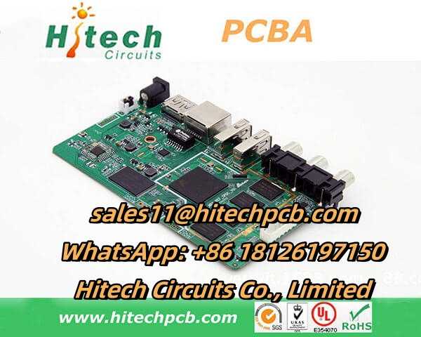
Briefly describe the basic process of PCBA patch processing
Briefly describe the basic process of PCBA patch processing <br> <br>The basic process of PCBA processing is to carry out SMT patch of components on the PCB board, DIP plug-in and realize welding. Here Hitech will briefly describe the basic process of PCBA processing for you. <br> <br>The PCBA processing process can be roughly divided into the following processes: SMT patch processing → DIP plug-in processing → PCBA testing → finished product assembly. <br> <br>1. SMT patch processing <br> <br>1). Solder paste stirring <br>The solder paste needs to be stirred before it can be used after it is taken out and thawed. <br> <br>2). Solder paste printing <br>The solder paste on the steel mesh is printed on the PCB pad by a scraper. <br> <br>3). SPI <br>SPI is the solder paste thickness detector. <br> <br>4). Mounting <br>The chip components are placed on the feeder, and the chip mounter head accurately mounts the components on the feeder on the PCB pad by identification. <br> <br>5). Reflow soldering <br>The mounted PCB board is reflowed to heat the solder paste into liquid and then cool and solidify to complete the welding process. <br> <br>6). AOI <br>AOI is automatic optical inspection, which detects the welding effect of PCB boards to eliminate bad PCB boards. <br> <br>7). Rework <br>Rework bad boards detected by AOI and manual inspection. <br> <br>2. DIP plug-in processing <br> <br>1). Plug-in <br>Insert the plug-in material on the PCB board. <br> <br>2). Wave soldering <br>The inserted board is soldered by wave soldering. <br> <br>3). Cutting the pins <br>The pins of the soldered board are generally too long and need to be cut. <br> <br>4). Post-welding processing <br>Use a soldering iron to manually solder the components. <br> <br>5). Washing the board <br>After wave soldering, the board will be dirty and needs to be cleaned with washing water and washing tank, or by machine. <br> <br>6). Quality inspection <br>Inspect the PCB board, unqualified products need to be repaired, and qualified products can enter the next process. <br> <br>3. PCBA testing <br> <br>According to different products and different customer requirements, different test methods are used to detect whether the PCBA products meet the PCBA processing requirements. <br> <br>4. Finished product assembly <br> <br>The PCBA products that have passed the test will be assembled into shells, and then tested. If the test is passed, it can be arranged for shipment. <br> <br>Hitech PCBA can provide you with high-quality SMT patch processing services, and also has rich PCBA processing experience. Hitech provide one-stop PCBA service for you. Hitech can also undertake DIP plug-in processing and PCB production, electronic circuit board manufacturing. <br> <br>If you have interest in our service, please feel freely contact Cynthia at sales11@hitechpcb.
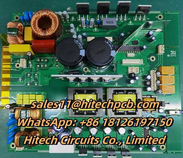
A brief introduction to the assembly and assembly process of PCB flip chip
A brief introduction to the assembly and assembly process of PCB flip chip <br> <br>Before discussing the assembly and assembly process of flip chips for PCB boards, it is necessary to understand what devices are called flip chips? In general, such devices have the following characteristics: <br> <br>1. The base material is silicon; <br> <br>2. Electrical surface and welding convex on the lower surface of the device; <br> <br>3. The ball spacing is generally 4-14mil, the ball diameter is 2.5-8mil, and the overall size is 1-27mm; <br> <br>4. After assembling on the substrate, you need to fill the bottom. <br> <br>In fact, the reason why the flip chip is called "flip" is relative to the traditional metal Wire Bonding connection method (Wire Bonding) and the process after planting the ball. The electrical side of the traditional chip connected to the substrate through metal wire bonding is facing up, and the electrical side of the flip chip is facing down, which is equivalent to turning the former over, so it is called "flip chip". After the chip is planted on the Wafer, it needs to be turned over and fed into the placement machine for easy mounting, and because of this flipping process, it is called "flip chip". <br> <br>First, PCB board with flip chip assembly process <br> <br>In the semiconductor back-end assembly plant, there are now two methods of module assembly. In the two reflow processes, SMT components are first assembled on a separate SMT line consisting of a screen press, a SMT mounter and the first reflow. The partially assembled modules are then processed through a second production line, which consists of PCB flip chip mounters and reflow furnaces. The bottom fill process is completed in a dedicated bottom fill line, or combined with a PCB flip chip line. <br> <br>Second, PCB board with flip chip assembly process introduction <br> <br>Compared with other IC devices, such as BGA, CSP, PCB flip chip assembly process has its special, the process introduces the flux process and the bottom filling process. Because of the flux residue (impact on reliability) and the danger of bridging, the PCB board is not an acceptable assembly method to mount on the solder paste with flip chips. In the industry, no cleaning flux was introduced, and the chip dipping flux process became a widely used welding aid technology. At present, the main alternative method is to use no-wash flux, dip the device in the flux film, dip the device ball into a certain amount of flux, and then mount the device on the substrate, and then reflow welding; Alternatively, the flux is pre-applied to the substrate, and then the device is mounted and reflow welded. The flux plays the role of fixing the device before reflow, and wetting the welding surface enhances the weldability during reflow. <br> <br>After the PCB board is welded with a flip chip, a glue (generally epoxy resin material) needs to be filled between the bottom of the device and the substrate. Bottom fill is divided into liquid and non-liquid (No-follow) bottom fill based on the "capillary flow principle". <br> <br>Flip chip assembly process flow (non-fluid bottom fill) <br> <br>The PCB flip-chip assembly process is for C4 devices (the device welding salient material is SnPb, SnAg, SnCu or SnAgCu). Another process is to use anisotropic conductive adhesive (ACF) to assemble PCB flip chips. The conductive adhesive is applied to the substrate in advance, and the device is mounted on the substrate with a higher pressure at the sticker head. At the same time, the device is heated to make the conductive adhesive solidify. This process requires a very high accuracy of the mounter, and a high pressure and heating function of the mounter head. For the assembly of non-C4 devices (whose convex material is Au or other), the trend is to use this process. Here, we mainly discuss the C4 process, and the following table lists several ways of Bumping PCB boards with flip chips and connecting on the substrate. <br> <br>A brief introduction to the assembly and assembly process of PCB flip chip <br> <br>The flip chip geometry of PCB board can be described by a "small" word: small ball diameter (as small as 0.05mm), small ball spacing (as small as 0.1mm), and small overall size (1mm2). In order to obtain satisfactory assembly yield, the mounting equipment and its process has brought challenges, with the reduction of the diameter of the welding ball, the mounting accuracy requirements are getting higher and higher, and the accuracy of 12μm or even 10μm is becoming more and more common. The graphics processing ability of the camera is also very critical, and the small ball diameter and small ball spacing require a higher pixel camera to process. <br> <br>Over time, the size of high-performance chips continues to increase, the number of Solder bumps increases, the substrate becomes thinner and thinner, and the bottom filling becomes necessary to improve product reliability. <br> <br>If you have interest, please feel free to contact me, Cynthia at [email protected].
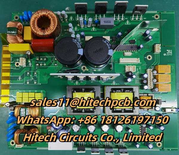
A brief introduction to the assembly and assembly process of PCB flip chip
A brief introduction to the assembly and assembly process of PCB flip chip <br> <br>Before discussing the assembly and assembly process of flip chips for PCB boards, it is necessary to understand what devices are called flip chips? In general, such devices have the following characteristics: <br> <br>1. The base material is silicon; <br> <br>2. Electrical surface and welding convex on the lower surface of the device; <br> <br>3. The ball spacing is generally 4-14mil, the ball diameter is 2.5-8mil, and the overall size is 1-27mm; <br> <br>4. After assembling on the substrate, you need to fill the bottom. <br> <br>In fact, the reason why the flip chip is called "flip" is relative to the traditional metal Wire Bonding connection method (Wire Bonding) and the process after planting the ball. The electrical side of the traditional chip connected to the substrate through metal wire bonding is facing up, and the electrical side of the flip chip is facing down, which is equivalent to turning the former over, so it is called "flip chip". After the chip is planted on the Wafer, it needs to be turned over and fed into the placement machine for easy mounting, and because of this flipping process, it is called "flip chip". <br> <br>First, PCB board with flip chip assembly process <br> <br>In the semiconductor back-end assembly plant, there are now two methods of module assembly. In the two reflow processes, SMT components are first assembled on a separate SMT line consisting of a screen press, a SMT mounter and the first reflow. The partially assembled modules are then processed through a second production line, which consists of PCB flip chip mounters and reflow furnaces. The bottom fill process is completed in a dedicated bottom fill line, or combined with a PCB flip chip line. <br> <br>Second, PCB board with flip chip assembly process introduction <br> <br>Compared with other IC devices, such as BGA, CSP, PCB flip chip assembly process has its special, the process introduces the flux process and the bottom filling process. Because of the flux residue (impact on reliability) and the danger of bridging, the PCB board is not an acceptable assembly method to mount on the solder paste with flip chips. In the industry, no cleaning flux was introduced, and the chip dipping flux process became a widely used welding aid technology. At present, the main alternative method is to use no-wash flux, dip the device in the flux film, dip the device ball into a certain amount of flux, and then mount the device on the substrate, and then reflow welding; Alternatively, the flux is pre-applied to the substrate, and then the device is mounted and reflow welded. The flux plays the role of fixing the device before reflow, and wetting the welding surface enhances the weldability during reflow. <br> <br>After the PCB board is welded with a flip chip, a glue (generally epoxy resin material) needs to be filled between the bottom of the device and the substrate. Bottom fill is divided into liquid and non-liquid (No-follow) bottom fill based on the "capillary flow principle". <br> <br>Flip chip assembly process flow (non-fluid bottom fill) <br> <br>The PCB flip-chip assembly process is for C4 devices (the device welding salient material is SnPb, SnAg, SnCu or SnAgCu). Another process is to use anisotropic conductive adhesive (ACF) to assemble PCB flip chips. The conductive adhesive is applied to the substrate in advance, and the device is mounted on the substrate with a higher pressure at the sticker head. At the same time, the device is heated to make the conductive adhesive solidify. This process requires a very high accuracy of the mounter, and a high pressure and heating function of the mounter head. For the assembly of non-C4 devices (whose convex material is Au or other), the trend is to use this process. Here, we mainly discuss the C4 process, and the following table lists several ways of Bumping PCB boards with flip chips and connecting on the substrate. <br> <br>A brief introduction to the assembly and assembly process of PCB flip chip <br> <br>The flip chip geometry of PCB board can be described by a "small" word: small ball diameter (as small as 0.05mm), small ball spacing (as small as 0.1mm), and small overall size (1mm2). In order to obtain satisfactory assembly yield, the mounting equipment and its process has brought challenges, with the reduction of the diameter of the welding ball, the mounting accuracy requirements are getting higher and higher, and the accuracy of 12μm or even 10μm is becoming more and more common. The graphics processing ability of the camera is also very critical, and the small ball diameter and small ball spacing require a higher pixel camera to process. <br> <br>Over time, the size of high-performance chips continues to increase, the number of Solder bumps increases, the substrate becomes thinner and thinner, and the bottom filling becomes necessary to improve product reliability. <br> <br>If you have interest, please feel free to contact me, Cynthia at [email protected].
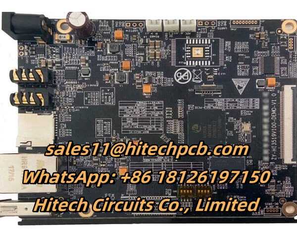
Understand the difference between PCB and PCBA
Understand the difference between PCB and PCBA <br> <br>I believe that many people are familiar with the PCB circuit board, and they may often hear about them in daily life, but they may not know much about the PCBA, and even will be confused with the PCB. So what is a PCB? How did PCBA evolve? What is the difference between PCB and PCBA? Let's take a look at it. <br> <br>About PCB <br> <br>PCB is short for Printed Circuit Board, because it is produced by electronic printing, it is called "printed" circuit board. PCB is an important electronic component in the electronics industry, it is the support body of electronic components and the carrier of electrical connection of electronic components. PCB has been extremely widely used in the manufacturing of electronic products, the reason why it can be widely used, its unique characteristics are summarized as follows: <br> <br>1. High wiring density, small size, light weight, which is conducive to the miniaturization of electronic equipment. <br> <br>2. Because the graphics are repetitive and consistent, the errors in wiring and assembly are reduced, and the maintenance, debugging and inspection time of equipment are saved. <br> <br>3. It is conducive to mechanized and automated production, improves labor productivity and reduces the cost of electronic equipment. <br> <br>4. The design can be standardized to facilitate interchangeability. <br> <br> <br>About PCBA <br> <br>PCBA is short for Printed Circuit Board + Assembly, that is to say, PCBA is through the SMT by empty PCB board, and then through the DIP plug-in of the entire process. <br> <br>Note: SMT and DIP are both ways of integrating parts on the PCB board, the main difference is that SMT does not require drilling on the PCB, and in DIP requires inserting the pin of the part into the already drilled hole. <br> <br>SMT - Surface Mounted Technology, the main use of the mounting machine is to mount some micro parts to the PCB board, its production process is: PCB board positioning, printing solder paste, mounting components, reflow and inspection. <br> <br>DIP is the "plug-in", that is, the insertion of parts on the PCB version, which is some parts that are larger in size and are not suitable for mounting technology when integrating parts in the form of plug-ins. Its main production process is: adhesive, plug-in components on the boards, inspection, wave soldering, brushing and finished inspection. <br> <br>* The difference between PCB and PCBA * <br> <br>From the above introduction, it can be known that PCBA generally refers to a processing process, which can also be understood as a finished circuit board, which can be counted as PCBA after the processes on the PCB board are completed. PCB refers to an empty printed circuit board with no parts on it. <br> <br>In general, PCBA is a finished board; The PCB is a bare board. <br> <br>If you have interest, please feel free to contact me, Cynthia at [email protected].
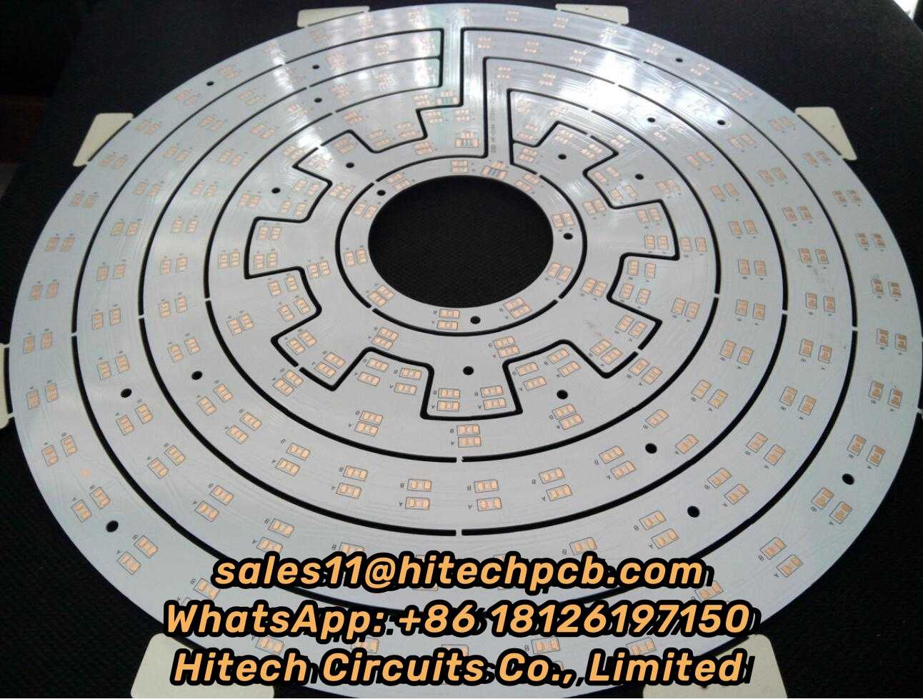
Different kinds of Aluminum PCBs
Different kinds of Aluminum PCBs <br> <br>Flexible Aluminum PCBs <br>One of the newest developments in IMS materials is flexible dielectrics. These materials feature a polyimide resin system with ceramic fillers which provides excellent electrical insulation, flexibility and of course thermal conductivity. When applied to a flexible aluminum material like 5754 or similar, the product can be formed to achieve a variety of shapes and angles which can eliminate costly fixtures, cables and connectors. Although these materials are flexible, they are intended to be bent into place and remain in place. They are not suited for applications that are intended to be flexed regularly. <br> <br>Hybrid Aluminum PCBs <br>In a ‘Hybrid’ IMS construction a “Sub-assembly” of a non-thermal material is processed independently and then bonded to the aluminum base with thermal materials. The most common construction is a 2-Layer or 4-Layer Sub-assembly made from conventional FR-4. Bonding this layer to an aluminum base with thermal dielectrics can help dissipate heat, improve rigidity and act as a shield. Other benefits include: <br>Less costly than a construction of all thermally conductive materials <br>Provides superior thermal performance over a standard FR-4 product <br>Can eliminate costly heat sinks and associated assembly steps <br>Can be used in RF applications where a surface layer of PTFE is desired for its’ loss characteristics. <br>Use of component windows in the aluminum to accommodate through-hole components. This allows connectors and cables to pass connections through the substrate while the solder fillet creates a seal without the need for special gaskets or other costly adapters. <br> <br>Multilayer Aluminum PCBs <br> Common in the high performance power supply market, multilayer IMS PCBs are made from multiple layers of thermally conductive dielectrics. These constructions have one or more layers of circuitry buried in the dielectric with blind vias acting as either thermal vias or signal vias. While more expensive and less efficient at transferring heat as a single layer designs, they provide a simple and effective solution for heat dissipation in more complex designs. <br> <br>Through-Hole Aluminum PCBs <br>In the most complex constructions a layer of aluminum can form a ‘Core’ of a multilayer thermal construction. The aluminum is pre-drilled and back-filled with dielectric prior to lamination. Thermal materials or sub-assemblies can be laminated to both sides of the aluminum using thermal bonding materials. Once laminated, the completed assembly is thru-drilled similar to a conventional multilayer PCB. The plated through holes pass through the clearances in the aluminum to maintain electrical insulation. Alternatively a Copper core can allow both direct electrical connections as well as with insulated through holes. <br> <br>If you want to know ceramic PCBs, please feel freely to contact Cynthia at [email protected]
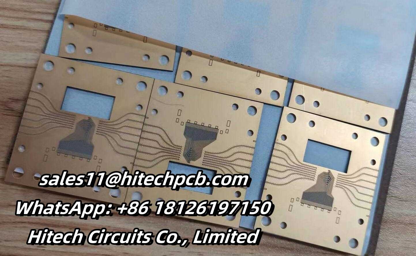
Why use ceramics for circuit boards?
Why use ceramics for circuit boards? <br> <br>Ceramic circuit boards are actually made of electronic ceramics material and can be made into various shapes. Among them, the ceramic circuit board has the most outstanding characteristics of high temperature resistance and high electrical insulation performance, and has the advantages of low dielectric constant and dielectric loss, high thermal conductivity, good chemical stability, and similar thermal expansion coefficient of the component, and Ceramic printed circuit boards are produced using LAM technology, a laser rapid activation metallization technology. Used in LED field, high power semiconductor module, semiconductor cooler, electronic heater, power control circuit, power mixing circuit, intelligent power component, high frequency switching power supply, solid state relay, automotive electronics, communication, aerospace and military electronics Component. <br> <br>Unlike traditional FR-4 (glass fiber) , ceramic materials have good high-frequency performance and electrical properties, and have high thermal conductivity, chemical stability and thermal stability. The ideal packaging material for a generation of large-scale integrated circuits and power electronics modules. <br> <br>Main advantages: <br> <br>1. Higher thermal conductivity <br> <br>2. be assembled in high density <br> <br>3. Good insulation <br> <br>4. The solder ability of the substrate is good and the use temperature is high <br> <br>5. More matching coefficient of thermal expansion <br> <br>6. Low frequency loss <br> <br>7. A harder, lower resistance metal film aluminum oxide ceramic circuit board <br> <br>8. Free of organic constituent, resistant to cosmic rays, high reliability in aerospace and long service life <br> <br>9. The copper layer does not contain an oxide layer and can be used for a long time in a reducing atmosphere. <br> <br>If you want to know ceramic PCBs, please feel freely to contact Cynthia at [email protected]
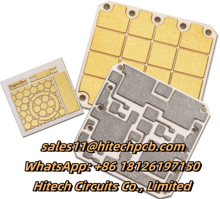
Aluminum Nitride Ceramic PCB
Aluminum Nitride Ceramic PCB <br>Aluminum Nitride Ceramic PCB have good high-frequency and electrical performance, and have high thermal conductivity, excellent chemical and thermal stability. Excellent corrosion resistance, it widely used in semiconductor and microelectronic circuit packaging pcb, High-brightness Led chip carrier board, automotive electronics and lighting components, high-power electronic component heat dissipation materials, etc. <br> <br> <br> <br>Technical Parameters <br>Aluminium Nitride (ALN) material <br>0.5mm Ceramic thickness <br>1 Oz Coppper thickness <br>ENEPIG suitable for gold wirebonding <br>Solder mask: White, Legend: Black <br>Laser Scribed <br>Application: Semi-Conductor <br> <br>If you want to know ceramic PCBs, please feel freely to contact Cynthia at [email protected]
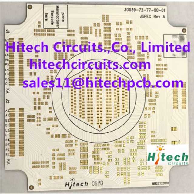
What is the difference between ceramic, high frequency and ordinary PCB boards?
What is the difference between ceramic, high frequency and ordinary PCB boards? <br> <br>Ceramic substrate is a kind of special PCB board with good thermal conductivity, insulation performance, and high dielectric constant. It is widely used in terminal products in the field of heat dissipation. Commonly used ceramic-based materials include aluminum oxide, aluminum nitride, zirconium oxide, ZTA, silicon nitride, silicon carbide, etc. FR circuit board refers to a circuit with epoxy glass fiber cloth as the main material. So, what is the difference between ceramic circuit board and ordinary PCB board <br> <br>1. The difference between ceramic substrate and PCB board <br> <br>a. Different materials. Ceramic substrate is an inorganic material, and the core is aluminum oxide or aluminum nitride; ordinary PCB board uses FR4 glass fiber board, which is an organic material. Ordinary PCB board can be laminated in multiple layers. LTCC is the mainstream of ceramic multilayer circuit board. The ceramic multilayer process currently being developed by Hitech Circuits Co., Ltd. is different from the traditional method. It uses magnetron sputtering technology to grow a layer of ceramic medium on the ceramic circuit board that has been metallized, and then re-metallizes this layer of medium to make the second layer of circuit. <br> <br>b. The performance and application of ceramic substrates are different. The thermal conductivity of ceramic substrates far exceeds that of ordinary PCB boards. The thermal conductivity of alumina ceramics is ≧25W(m·K), and the thermal conductivity of aluminum nitride ceramics is ≧170W(m·K). They are used in industries with large heat dissipation requirements, such as high-power LED lighting, high-power modules, high-frequency communications, and track power supplies. The thermal expansion coefficient of ceramic substrates is more compatible with silicon wafers, and the product stability is higher. Ordinary PCB boards are widely used, mostly in private commercial products. <br> <br>2. The difference between ceramic substrates and high-frequency boards <br> <br>a. Different materials. Ceramic substrates are made of aluminum oxide or aluminum nitride, while high-frequency boards are mostly made of Rogers, Yalong, polytetrafluoroethylene, etc., with low dielectric constants and fast high-frequency communication speeds. <br> <br>b. Different performance. Ceramic substrates are widely used in cooling sheets and systems, high-power modules, automotive electronics and other fields. High-frequency PCB boards are mainly used in high-frequency communications, aviation, high-end consumer electronics, etc. <br> <br>3. In the field of high-frequency communications involving heat dissipation requirements, ceramic substrates are usually required to be combined with high-frequency PCB boards, such as high-frequency ceramic PCBs. <br> <br>If you want to know ceramic PCBs, please feel freely to contact Cynthia at [email protected]
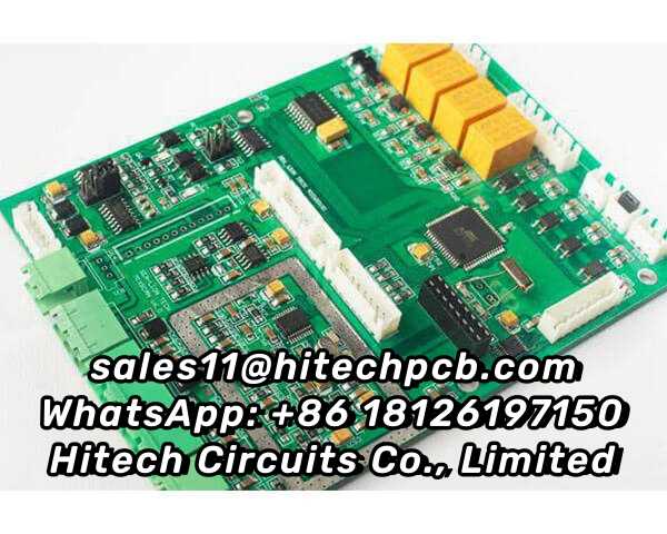
How to reduce Ground Bounce Reduction on PCBAs
How to reduce Ground Bounce Reduction on PCBAs <br>1. Minimize return paths <br> <br>The shorter the return paths, the lower the inductance between components and the ground plane. Therefore, digital components should be placed directly over digital ground areas and mixed-signal devices should be positioned above bridges between digital and analog ground areas, whenever possible. <br> <br>2. Use short component leads <br> <br>Using packages with shorter component leads reduces the series inductance. This is also accomplished by using BGAs and vias. Decoupling capacitors should also be used to funnel disturbances to ground as quickly as possible. It is probably a good idea to use these for all IC and transistor ground pins. <br> <br>3. Use multiple vias <br> <br>Another way to quickly dissipate disturbances or noise from your circuits is to use multiple vias to route to ground. <br> <br>4. Offset switching, if possible <br> <br>The parasitics that cause ground bounce may not be able to be completely eliminated; however, by offsetting switching times, you can minimize the extent or magnitude of the ground bounce. <br> <br>5. Use slower switching components, if possible <br> <br>This technique should be used in conjunction with offsets to allow damping to occur prior to the next switching event. This will prevent it from being added to the noise that may be already present.
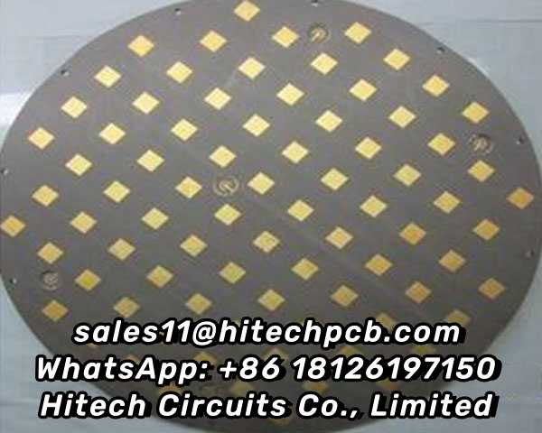
5 Tips to choose an ideal Ceramics Manufacturer
5 Tips to choose an ideal Ceramics Manufacturer <br> <br>Ceramic printed circuit boards are causing a storm in the electrical industry. With a wide range of uses in different electrical devices, its ease of use, cost, durability, and versatility makes it one of the most sorted PCBs in the market. However, because of highlighted benefits, it has become increasingly difficult to choose the right ceramic PCB manufacturer to invest in. Below are things you should consider before you pick your ceramic PCB manufacturer. <br> <br>High quality <br>As expected, choosing a PCB manufacturer that assures you of high-quality products should be your priority. Ideally, a good manufacturer is one that provides you with a board that has no errors. When choosing, take an interest in the ceramic PCB manufacturing process as it will alert you to their business perception. This includes the ability to deliver boards that have the right dimensions, accurately drilled holes, high consistency, and ability to pass the bare board test. <br> <br>Ability to meet requirements <br>When looking for multilayer ceramic PCB manufacturers, getting confused by their jargons can be easy. Make it easier by asking them if they can meet your specific requirements. Gauge them by how they will react to inquiring of the standardized formats. Research how they delivered a previous clients request of production of ceramic PCB type and remember to focus on any special offers granted. <br> <br>PCB manufacture cost <br>When considering a printed circuit board ceramic PCB manufacturer examine the cost of their services. Ideally, cost reduction with large orders is a good enough reason to settle for a manufacturer. However, when doing so ensure that they offer high-quality products. Overall, it’s better to choose a pricier manufacturer who assures you of high quality than settle for a great deal that offers low-quality PCB. <br> <br>Materials sourcing <br>To fully enjoy the various benefits of ceramic PCB advantages take time to consider where they get their materials from. A manufacturer that aims to source from the cheapest place will assure you of a low cost of production. However, with this comes the risk of attaining low material quality as they sacrifice quality for quantity. The right PCB manufacturer will have a select number of places to sort their materials hence provide consistently high-quality PCB from batch to batch. <br> <br>Board testing <br>Before you settle and decide to purchase anything long lasting investment, a test drive is always recommended. A good PCB manufacturer will give you the opportunity to test out their boards, possibly under random sample basis. This allows you to check if their product conforms to required standards. When choosing a ceramic PCB manufacturer, aim to pick one that offers you this opportunity to avoid disappointments later on.
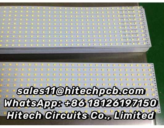
3 Main Types of PCB Materials
3 Main Types of PCB Materials <br>The primary material used to fabricate PCB (Printed Circuit Board) is of immense importance. It is essential to consider the performance of the material in terms of temperature resistance, adhesion, tensile strength, flexibility, dielectric strength, dielectric constant, and many other physical, electrical, and thermal factors. The performance and level of integration of the PCB is completely dependent on the material used to fabricate the PCB. <br> <br>Types of Materials Used for PCB Fabrication <br> <br>There are three major types of materials used for production of PCB: <br>1. FR-4 : This is the most commonly used material in PCB. It is a glass reinforced epoxy laminate sheet. The epoxy used is flame retardant and water resistant. It provides good strength to weight ratios. The tensile strength offered by this material is very high. <br>2.PTFE (Teflon): PTFE is a kind of plastic material that does not provide any resistance, thus is used for high speed, high frequency applications. PTFE is extremely flexible, making it invaluable in applications with tight tolerances. It is also extremely lightweight, allowing it to be used across various industries. It is also flame resistant, exhibits high physical strength, provides temperature stability, and is versatile in application. <br>3.Metal :The traditional materials of copper, aluminum, iron, etc. are still used in PCBs. These materials allow the use of Surface Mount Technology (SMT) for the integration of components. They also provide mechanical durability. Thus, the product life of metal base PCBs is much longer. <br> <br>The different materials used for the fabrication of PCB, all offer a variety of advantages and disadvantages. The material is chosen according to the application, the result needed, environmental factors, and any other constraints the PCB will face. You should choose the material of the PCB depending on the results that are expected.
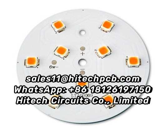
4 Advantages and 8 Applications of Aluminum PCB
4 Advantages and 8 Applications of Aluminum PCB <br> <br>Stack-layer of Singe Aluminum PCB <br> <br>It features a thermal clad layer that dissipates heat in a highly efficient manner, while cooling components and increasing the overall performance of the products. <br> <br>Advantages of Aluminum PCB <br> <br>1. Environmentally Friendly: Aluminum is non-toxic and recyclable. Manufacturing with aluminum is also conducive to conserving energy due to its ease of assembly. For printed circuit board suppliers, using this metal helps maintain the health of our planet. <br> <br>2. Heat dissipation: High temperatures can cause severe damage to electronics, so it is wise to use a material that can help dissipate heat. Aluminum can actually transfer heat away from vital components, thus minimizing the harmful effect it could have on the circuit board. <br> <br>3. Higher durability: Aluminum provides strength and durability to a product that ceramic or fiberglass bases cannot provides. Aluminum is a sturdy base material that can reduce accidental breakage during manufacturing, handling, and everyday use. <br> <br>4. Lightweight: For its incredible durability, aluminum is a surprisingly lightweight metal. Aluminum adds strength and resilience without adding on any additional weight. <br> <br> <br>8 Applications of Aluminum PCB <br> <br>1. Audio device: Input, output amplifier, balanced amplifier, audio amplifier, pre-amplifier, power amplifier. <br> <br>2. Power Supply: Switching regulator, DC / AC converter, SW regulator, etc. <br> <br>3. Communication electronic equipment: High-frequency amplifier, filtering appliances, transmitter circuit <br> <br>4. Office automation equipment: Motor drive, etc. <br> <br>5. Automobile: Electronic regulator, ignition, power supply controller, etc. <br> <br>6. Computer: CPU board, floppy disk drive, power supply devices, etc. <br> <br>7. Power Modules: Inverter, solid state relays, rectifier bridges. <br> <br>8. Lamps and lighting: As the advocated promotion of energy-saving lamps, a variety of colorful energy-saving LED lights are well received by the market, and aluminum pcb used in LED lights also begin large-scale applications.
About Cynthia_HitechPCB_manufacturing Hitech Circuits PCB's Store
No description provided.
0.0
Customer Reviews
See what others are saying about Cynthia_HitechPCB_manufacturing Hitech Circuits PCB's Store. We verify purchases to ensure reviews are genuine.
No reviews yet for this store.