PCB Board Layout: A Complete Guide to Efficient Circuit Design
Designing a printed circuit board (PCB) is a critical step in modern electronics development. A well-planned pcb board layout ensures optimal performance, reliability, and manufacturability of electronic devices. Whether you're working on consumer electronics, industrial systems, or embedded solutions, understanding layout principles is essential.
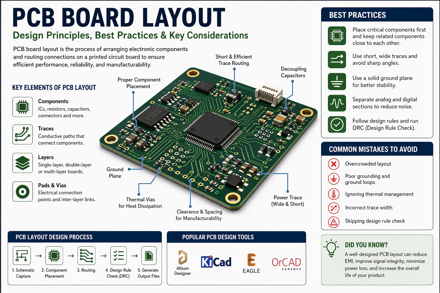
Understanding PCB Board Layout
A PCB layout refers to the physical arrangement of electronic components and the routing of electrical connections on a board. It transforms a schematic diagram into a manufacturable design.
Key Elements of a PCB Layout
- Components: Resistors, capacitors, ICs, and connectors
- Traces: Conductive paths connecting components
- Layers: Single-layer, double-layer, or multi-layer boards
- Pads and vias: Connection points and inter-layer links
A well-executed layout reduces signal interference, improves thermal performance, and enhances durability.
Importance of PCB Board Layout in Electronics
A poorly designed layout can lead to performance issues, signal noise, or even complete circuit failure. On the other hand, an optimized PCB board layout ensures:
- Stable electrical performance
- Reduced electromagnetic interference (EMI)
- Efficient heat dissipation
- Easier manufacturing and assembly
- Lower production costs
In high-speed or sensitive applications, layout decisions can significantly impact product success.
Tools Used for PCB Board Layout Design
Modern PCB design relies on advanced software tools that simplify complex tasks.
Popular PCB Design Software
- Altium Designer – Professional-grade design platform
- KiCad – Open-source and widely used
- Eagle – Beginner-friendly with strong community support
- OrCAD – Advanced simulation and design capabilities
These tools provide features like schematic capture, layout editing, and design rule checking (DRC).
Features to Look For
When choosing a tool, consider:
- User-friendly interface
- 3D visualization capabilities
- Simulation and testing features
- Library of components
- Manufacturing output support (Gerber files)
Common Mistakes to Avoid in PCB Layout
Even experienced designers can encounter challenges. Avoiding common errors improves design quality.
Frequent Design Errors
- Overcrowded component placement
- Inadequate grounding
- Ignoring thermal management
- Improper trace width
- Skipping design rule checks
How to Prevent Issues
- Perform regular design reviews
- Use automated DRC tools
- Follow manufacturer guidelines
- Prototype and test early
Attention to detail can save time and reduce costly redesigns.
Advanced Considerations for PCB Layout
As designs become more complex, additional factors must be considered.
High-Speed Design
For high-frequency circuits:
- Maintain controlled impedance
- Use differential pair routing
- Minimize signal reflections
Thermal Management
Efficient heat handling ensures longevity.
- Use thermal vias
- Add heat sinks where needed
- Optimize airflow in enclosure design
Multi-Layer PCB Design
Multi-layer boards improve performance but require careful planning.
- Separate signal, power, and ground layers
- Reduce electromagnetic interference
- Improve signal integrity
Conclusion
A well-designed pcb board layout is essential for creating reliable and high-performing electronic products. From proper component placement to advanced routing techniques, every detail plays a role in the final outcome.