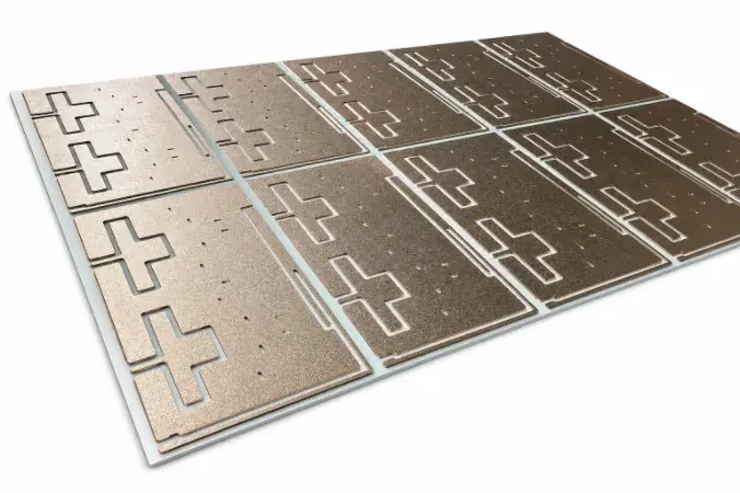
Ceramic PCB Manufacturer for Advanced Electronics
Choosing the right ceramic PCB manufacturer is important for electronic products that require efficient heat management, electrical insulation, mechanical stability, and specialized circuit construction. Ceramic PCBs are often considered for demanding applications where conventional PCB materials may not provide the required combination of thermal and electrical properties.
Ceramic PCB manufacturing starts with selecting the appropriate substrate and metallization method. Common options include alumina, aluminum nitride (AlN), DBC, DPC, thick-film, and LTCC constructions. Each route has different characteristics, so the best choice depends on the thermal path, circuit geometry, copper requirements, package interface, and operating conditions. HLCPCB lists 96% alumina as a standard screening material and identifies AlN and LTCC as advanced construction options requiring project review.
Selecting the Right Ceramic Substrate
Alumina can be suitable for many general ceramic circuit applications where its thermal, electrical, mechanical, and cost characteristics meet the product requirements. Aluminum nitride can be considered when the thermal model or package expansion requirements call for a different material system.
Material selection should not be based on thermal conductivity alone. Ceramic thickness, copper spreading, attachment layers, mounting conditions, cooling method, package materials, and operating temperature all influence the performance of the finished assembly. HLCPCB specifically notes that material datasheet values should not be treated as guaranteed finished-board thermal performance.
Choosing the Metallization Process
The metallization route should match the electrical and mechanical requirements of the design. Direct Bonded Copper, or DBC, is commonly considered for heavier copper and power-oriented structures. Direct Plated Copper, or DPC, can support finer conductor geometries and plated structures. Thick-film technology is suited to printed conductors and functional pastes, while LTCC can be used for specialized multilayer ceramic integration.
These processes are not interchangeable. Copper thickness, trace and space, via structures, pad geometry, ceramic thickness, flatness, and assembly requirements must be evaluated together before the manufacturing process is finalized.
Thermal Performance and Mechanical Design
One of the major reasons companies consider ceramic PCBs is thermal management. However, the ceramic substrate is only one part of the complete thermal path. Engineers should consider the heat source, copper distribution, ceramic thickness, die attachment, thermal interface material, mounting pressure, heat sink, airflow, and cooling conditions.
Mechanical stress is equally important. Different materials expand at different rates as temperature changes. The ceramic substrate, copper, semiconductor die, package, attachment materials, and enclosure should therefore be evaluated together, particularly for products that experience repeated thermal cycling.
Manufacturing and Quality Control
A reliable ceramic PCB production process requires complete technical information. Gerber or ODB++ files, mechanical drawings, substrate specifications, copper thickness, holes, vias, dimensions, flatness requirements, surface finish, and assembly details can help a manufacturer evaluate the proposed construction.
Inspection requirements should also be defined before production. Depending on the application, these may include automated optical inspection, electrical testing, dimensional inspection, bond-related checks, thermal testing, or other specialized verification. The exact inspection scope should be agreed as part of the quotation and manufacturing requirements.
Applications of Ceramic PCBs
Ceramic substrates can be considered for power electronics, RF equipment, sensors, automotive systems, industrial controls, LED applications, semiconductor packages, and other advanced electronic products. The appropriate construction depends on the actual product requirements rather than simply the application category.
For example, a power module may prioritize heavy copper and thermal transfer, while an RF or sensor design may place greater emphasis on fine conductor geometry and controlled electrical characteristics. A multilayer package with embedded structures may require an LTCC-based solution instead.
Planning a Successful Ceramic PCB Project
Before requesting production, engineers and purchasing teams should define the ceramic grade, supplier specification, metallization route, copper or conductor thickness, circuit geometry, dimensions, surface finish, assembly interface, thermal requirements, operating temperature, testing, quantity, and delivery expectations.
A capable manufacturer can then review these requirements as one complete construction instead of evaluating each specification separately. This helps prevent incompatible combinations, such as applying fine-line requirements to a construction designed for very thick copper.
Ultimately, selecting an experienced ceramic PCB manufacturer is about matching the material, metallization process, circuit geometry, thermal path, mechanical design, and quality requirements to the finished product. Careful engineering review before production can create a more predictable manufacturing process and provide a stronger foundation for both prototype development and future production.


